Photonics Research, 2020, 8 (10): 10001551, Published Online: Sep. 11, 2020  

Widely tunable, heterogeneously integrated quantum-dot O-band lasers on silicon Download: 745次

Author Affiliations
1 Department of Electrical & Computer Engineering, University of California, Santa Barbara, California 93106, USA
2 Nexus Photonics, Goleta, California 93117, USA
3 Hewlett Packard Labs, Palo Alto, California 94304, USA
Abstract
Heterogeneously integrated lasers in the O-band are a key component in realizing low-power optical interconnects for data centers and high-performance computing. Quantum-dot-based materials have been particularly appealing for light generation due to their ultralow lasing thresholds, small linewidth enhancement factor, and low sensitivity to reflections. Here, we present widely tunable quantum-dot lasers heterogeneously integrated on silicon-on-insulator substrate. The tuning mechanism is based on Vernier dual-ring geometry, and a 47 nm tuning range with 52 dB side-mode suppression ratio is observed. These parameters show an increase to 52 nm and 58 dB, respectively, when an additional wavelength filter in the form of a Mach–Zehnder interferometer is added to the cavity. The Lorentzian linewidth of the lasers is measured as low as 5.3 kHz.

1. INTRODUCTION

The rise in datacenter traffic is creating a demand for low-cost, low-power consumption, highly reliable optical transceivers. Silicon photonics is the only technology that can meet such demands. In the last decade, silicon photonic integrated circuits (PICs) have shown tremendous growth and have transitioned from research labs to products [1]. Today, silicon PICs are fabricated in state-of-the-art 300 mm pilot lines on silicon-on-insulator (SOI) wafers and take advantage of the highly mature fabrication processes developed for electronic integrated circuits (EICs). A key differentiating point between PICs and EICs is that the feature size for PICs does not scale with advanced nodes (e.g., the single-mode width of the waveguide is always the same). However, access to advanced technology nodes reduces defect density and process-dependent variations in silicon PICs. Since the advanced technology nodes are already developed for EICs, separate development for PICs is not needed thus saving costs. As a result, several foundry services are available across the globe that provide silicon PICs in the O-band (centered around 1310 nm) and the C-band (centered around 1550 nm). Low-loss waveguides and passive devices such as wavelength filters (ring resonators, Mach–Zehnder interferometers) and wavelength (de)multiplexers (arrayed waveguide gratings) are available in the portfolio of these foundries. Active devices in silicon PICs have also been realized by fabricating p-n junctions to form modulators or by depositing epitaxial germanium film to form detectors [2].

The only drawback for silicon PICs is the lack of a light source on account of silicon being an indirect bandgap material. On the other hand, III–V materials allow bandgap engineering, and light emission by electrical injection can be achieved. Quantum dots (QDs) are particularly attractive light emitters due to their atom-like density of states. This allows engineering of gain bandwidth and the peak emission wavelength by changing dot growth conditions [3]. QDs have a low linewidth enhancement factor (αH), which allows reducing the laser linewidth. Additionally, QD-based lasers are more insensitive to both feedback and defect density in comparison with quantum well (QW) lasers [4]. Therefore, integration of QD lasers on silicon PICs promises to bring the entire high-performing transceiver circuit on a single chip.

Two approaches to integrate QD lasers on silicon PICs are compatible with the wafer-scale process: epitaxial growth and heterogeneous integration. There has been extensive research on epitaxial growth of QD material on silicon substrates [57" target="_self" style="display: inline;">–7], which requires careful optimization of a thick buffer layer to control the dislocation density. Defect densities on the order of 106  cm2 have been achieved, which results in nearly identical performance of QD lasers grown on silicon and grown on a GaAs substrate [8]. Another crucial parameter for optimal device performance is the reduction of recombination enhanced dislocation climb. Improvements in growth conditions of QD lasers on silicon have resulted in high injection efficiency (87%) and degradation of free operation with an extrapolated lifetime of over 10 million hours [9]. In an ideal case, the QD lasers grown on silicon would couple light into the underlying silicon waveguide. There have been reports demonstrating growth of QD lasers on SOI substrates [10], but the substrates require III–V material growth in patterned V-grooves to minimize defects using aspect ratio trapping. Even these lasers are not coupled to silicon waveguides and work only under optical injection. Therefore, further work is needed to develop the technology to achieve light coupling into silicon waveguides.

On the other hand, heterogeneous integration provides an attractive way of placing III–V gain material on SOI wafers. In this approach, III–V gain materials are bonded to a pre-patterned SOI wafer and then processed after substrate removal to form laser structures. Thanks to the similar refractive indices between III–V and silicon, light is efficiently transferred from the gain provided by III–V layer to passive silicon waveguides via adiabatic taper structures defined lithographically. Heterogeneous integration is a mature technology with 300 mm volume production feasibility, and several industrial players, e.g., Intel, Juniper Networks, and HPE, are producing or developing commercial transceivers based on it [1,11]. Silicon-nitride-based waveguides present an alternate to SOI waveguides and have ultralow loss [12]. External cavity narrow linewidth lasers have been realized using the hybrid [13] (where two chips are butt-coupled to each other) and heterogeneous approaches [14]. The hybrid approach is not scalable to wafer-level processing, and the heterogeneous approach requires multilevel wafer bonding, which has not yet been developed commercially. Additionally, due to low index contrast, silicon-nitride waveguide circuits have a large footprint compared with SOI waveguides. Therefore, heterogeneously integrated QD lasers on SOI wafers are the most promising candidates for reduced cost and size and more simple transceivers.

Several reports of single-mode lasers integrated on silicon, using both epitaxial growth and heterogeneous integration, working in the O-band have been published, including distributed feedback (DFB) lasers and tunable lasers. While DFB lasers can only be tuned within a few nm range, tunable lasers with wide-tuning range allow maintaining a flexible grid and reduce power consumption in tuning other transceiver network elements. This is essential in datacenters where a large number of transceivers are deployed.

In this paper, we report the first demonstration of widely tunable QD lasers heterogeneously integrated on SOI wafers operating in the O-band. Table 1 compares the results obtained in this work with other lasers on silicon (both epitaxially grown and heterogeneously integrated) operating in the O-band in terms of threshold current (Ith), tuning range (Δλ), side-mode suppression ratio (SMSR), and linewidth. It is worth mentioning that a delayed self-heterodyne method is used in Ref. [15] to measure the linewidth, while other linewidths were extracted from laser frequency noise spectra. Our results are on par with other published results in terms of Ith and tuning range and show an improvement in terms of SMSR and spectral linewidth. These results are particularly appealing for coherent communications, where all research and commercial receivers use an isolator between the local oscillator and the coherent receiver, which has prevented integration onto a single chip. Coherent transceivers have not been deployed in datacenters and other cost-sensitive applications for this reason. The laser described in this paper will enable isolator-free operation of the coherent datacenter interconnects, as the heterogeneously integrated QD laser and the silicon photonics transceivers can be integrated on the same chip. This has not been possible using previously demonstrated quantum well lasers due to their higher sensitivity to reflections, which require an isolator between the laser and the transceiver [4,22].

Table 1. Comparison of O-Band Single Wavelength Lasers on Silicon

Laser TypeIth(mA)Δλ(nm)SMSR (dB)Linewidth (kHz)
Epitaxial Growth
DFB [16]12NA50NA
Tunable [17]331645NA
Tunable [18]465.435716
Heterogeneous Integration
DFB [19]9.5NA47NA
Vernier ring [15]30544550
Interferometric [20]9.53040NA
SGDBR [21]1003535NA
This work3052585.3

查看所有表

2. LASER DESIGNS AND FABRICATION

The single-mode lasing is achieved by using two ring resonators in a Vernier scheme, where the two silicon passive rings have a slightly different free spectral range (FSR). This leads to an increase in the total FSR of the two-ring system allowing for wide tuning range. This scheme is employed to realize tunable lasers in several wavelength bands [23,24]. The III–V/silicon gain region is located between two mirrors. The back mirror consists of two ring resonators with the same waveguide width (500 nm) and slightly different radii (40 μm and 41.2 μm). The targeted FSR of each ring resonator is 1.746 and 1.683 nm, which gives a total Vernier FSR of 46.14 nm. The gap between the bus waveguide and the ring resonator is fixed at 265 nm, which corresponds to a 9% coupling coefficient. The front mirror is formed by a Sagnac loop, which is designed for 40% reflection. The 40% reflectivity of the front facet is a conservative value chosen to ensure we obtain enough reflections to compensate for cavity losses. This value can be improved in future-generation devices to achieve a balance between threshold current density and output optical power. The output from the front mirror is fed into a 2×2 multimode interferometer (MMI) designed with a 15:85 splitting ratio. The 15% output of the MMI is connected to an on-chip avalanche photo-diode (APD) [25], and the 85% output is connected to a grating coupler. The insertion loss of the grating coupler was measured to be 10.5 dB. A silicon waveguide phase section is also included between the front mirror and the gain region for aligning the laser cavity modes with the ring modes. Both rings and the phase section have metal resistive heaters on them for thermo-optic tuning.

To increase the SMSR, a third filter in the form of a tunable Mach–Zehnder interferometer (MZI) is added to the Vernier ring geometry. The path length difference of the MZI is chosen such that the MZI FSR is twice the average ring FSR, so as to suppress the neighboring Vernier modes. More details on the operation principle of this device are discussed in Ref. [26]. A schematic diagram of both devices is shown in Figs. 1(a) and 1(b), respectively.
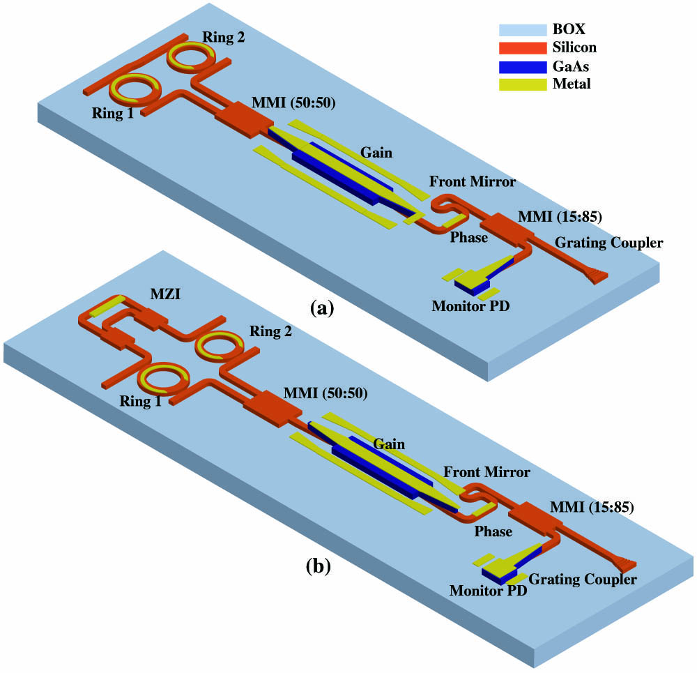
Fig. 1. Schematic diagram of (a) two-ring Vernier and (b) two-ring Vernier with MZI tunable laser. Electrical contacts are shown in gold.

下载图片 查看所有图片

The devices were fabricated on 100 mm wafers using the fabrication process described in Ref. [27]. The SOI wafer has a 400 nm thick silicon device layer and a 2 μm buried oxide layer. The gain material has a GaAs-based p-i-n structure with 8 QD layers. The gain region is 1.4 mm long, and the active region is 4 μm wide.

3. LASER CHARACTERIZATION

The devices were characterized on a temperature-controlled stage at 20°C. Electrical contacts were made using a probe card, and the output fiber was positioned using a closed-loop piezo electric stage. The output fiber was connected to an optical isolator followed by a 1:99 splitter. The 1% output was fed to a fiber alignment controller (Thorlabs K-Cube Nanotrak NIR), which monitors the piezo controls. The 99% output was connected to a 50:50 splitter feeding into a wave meter (Yokogawa AQ6150) and a power meter (Agilent 81635A). For subsequent tuning map measurements, the power meter was replaced by an optical spectrum analyzer (Yokogawa OSA AQ6370D). For linewidth measurements, the output going to the 50:50 splitter was instead connected to a polarization controller and polarization beam splitter (PBS), which was then connected to an OE waves linewidth measurement tool (OE4000). The other port of the PBS was fed to the OSA to monitor the SMSR.

3.2 A. Light–Current–Voltage Characteristics

The light–current–voltage (LIV) characteristics were obtained by sweeping the current in the gain region while monitoring the power collected in the fiber through the grating coupler. Figure 2(a) shows the measured LIV characteristics of the Vernier ring laser. The threshold is found to be 20 mA (corresponding to a threshold current density, Jth of 357  A/cm2), and several mode hops can be seen at various drive currents. To understand these mode hops, we also looked at the lasing wavelength while sweeping the laser drive current. Fiber-coupled light is analyzed with an optical spectrum analyzer (OSA) and a wave meter. Figure 2(b) shows two types of mode hops present in our laser cavity. The first type is the mode hops between the ring cavity modes, which are spaced 1.6592 nm apart, agreeing well with our design. The second type is the hops between the longitudinal cavity modes spaced 57.72 pm apart. For realizing a mode-hop-free operation, both the ring modes and the cavity modes need to be tuned together. Another interesting feature of the LIV curve can be seen above 260 mA drive current. A decrease in output light is observed; however, this is not due to thermal roll-off. Instead, we observe excited state lasing at these high drive currents. Figure 2(c) shows the OSA trace taken at 290 mA drive current. The main lasing peak can be observed at 1297.3 nm, while the excited state lasing peak is observed at 1203.1 nm. This is an interesting feature of our QD device, as it provides access to a much wider wavelength range. While this manuscript is exclusively focused on lasing behavior in the ground state, observance of the excited state at a higher drive current does open up additional avenues for our device, including broader modulation bandwidth [28] and shorter pulse duration while operating as a mode-locked laser [29,30].
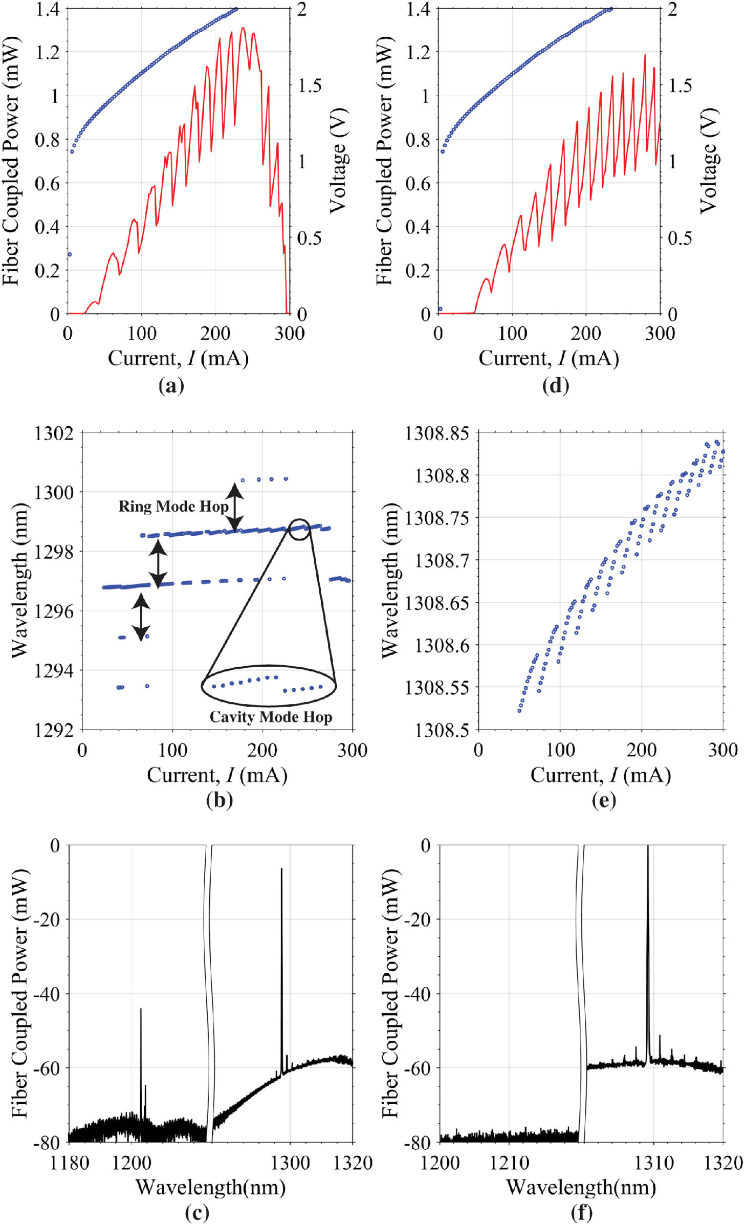
Fig. 2. (a) LIV characteristics of the Vernier ring laser when both rings are unbiased. (b) Spectral characteristics showing ring mode hops and cavity mode hops. (c) OSA trace at 290 mA drive current (curve has been truncated in the middle) showing both ground state and excited state lasing can be observed. (d) LIV characteristics of the Vernier ring laser when ring one is unbiased and ring two has 45.8 mW electrical power applied. (e) Spectral characteristics showing only cavity mode hops. (f) OSA trace at 290 mA drive current showing only ground-state lasing.

下载图片 查看所有图片

It is possible to operate the device in a pure ground state by optimally aligning the Vernier rings, allowing only a single reflection peak in the O-band. Figure 2(d) shows the LIV characteristics when no electrical power is applied to the first ring and 45.2 mW electrical power is applied to the second ring. The threshold current increases to 50 mA; however, there is no power roll-off at higher drive currents, and only cavity mode hops are observed, as shown in Figs. 2(c) and 2(d). The OSA trace taken at 290 mA drive current shown in Fig. 2(e) confirms that the ground state lases at 1309.2 nm, while the excited state does not.

The LIV characteristics of the Vernier ring MZI laser are shown in Fig. 3(a). The threshold current is found to be 35 mA with 2.2 mW optical power coupled to the fiber, equivalent to 29 mW on-chip output power. Even when no electrical power is applied to the rings and the MZI, only cavity mode hops are observed [Fig. 3(b)], indicating that the reflection spectrum from the back mirror is aligned properly with the gain peak. Only ground state lasing is observed in this condition, and no roll-off is seen.
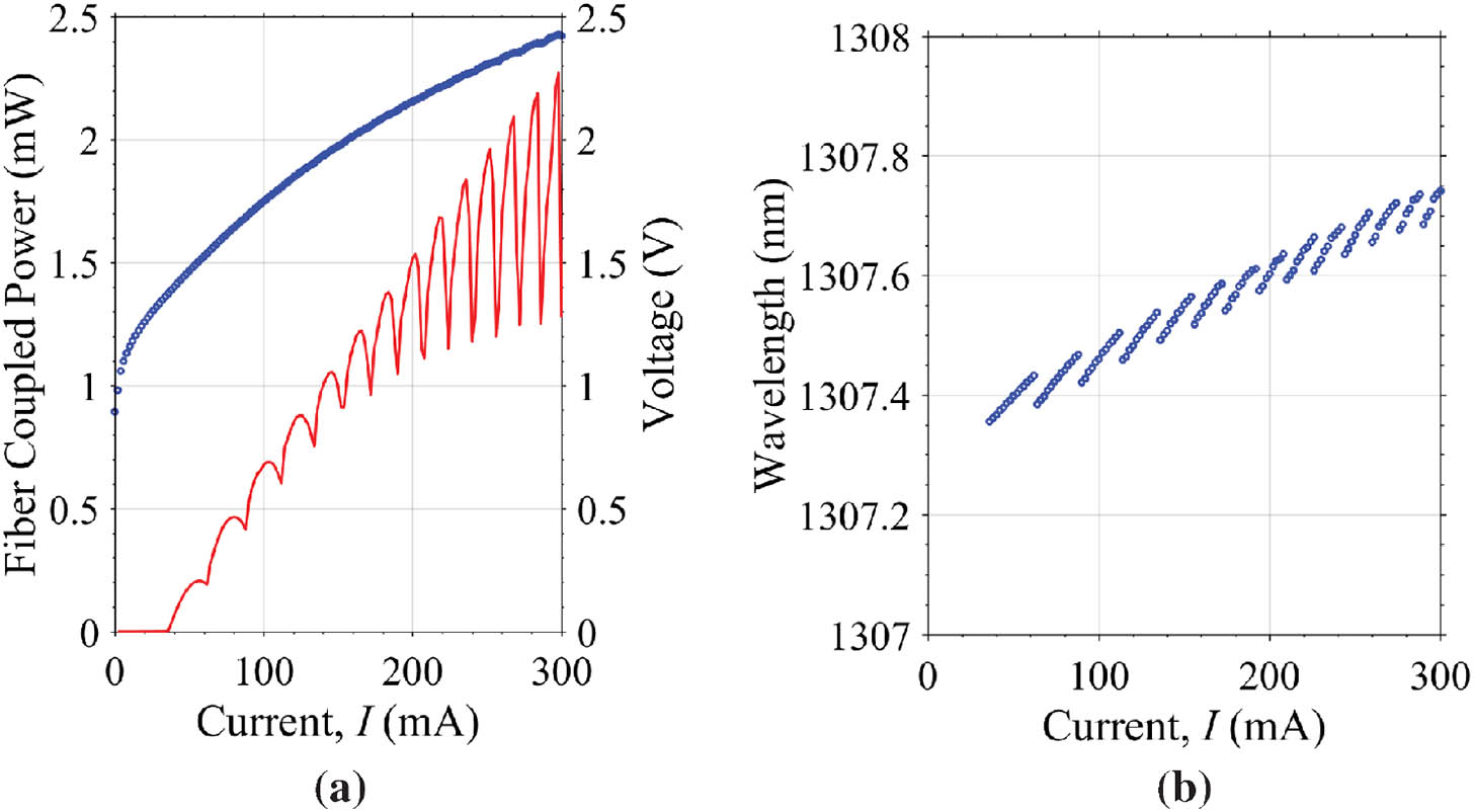
Fig. 3. (a) LIV characteristics of the Vernier ring MZI laser. (b) Spectral characteristics showing cavity mode hops.

下载图片 查看所有图片

The longitudinal mode spacing is used to calculate the total cavity length (3.812 mm for Vernier ring case and 4.741 mm for Vernier ring MZI case), which provides an estimate of the coupling coefficient (0.18 and 0.24, respectively). These higher coupling coefficients point toward a 50 nm smaller than designed gap between the waveguide and the rings.

3.3 B. Wavelength Tuning

The location of the lasing wavelength is determined by the reflection peak of the Vernier rings. Either of the rings can be tuned to choose the lasing wavelength. This effect is shown in Figs. 4(a) and 4(b) for the first and second ring, respectively. Increasing the heater power on the first ring introduces a redshift in the lasing peak, while a blueshift is observed when the second ring is tuned. The power required to obtain a 2π phase shift for the first and second ring is 51 and 47.5 mW, respectively. This individual tuning of each ring provides us with an approximation on the total tuning range of the laser.
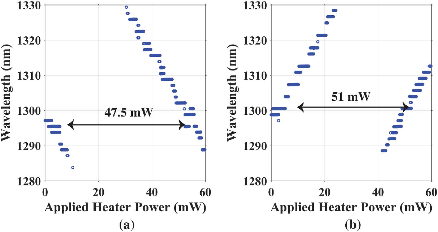
Fig. 4. Lasing wavelength as a function of the applied heater power for (a) the first ring and (b) the second ring.

下载图片 查看所有图片

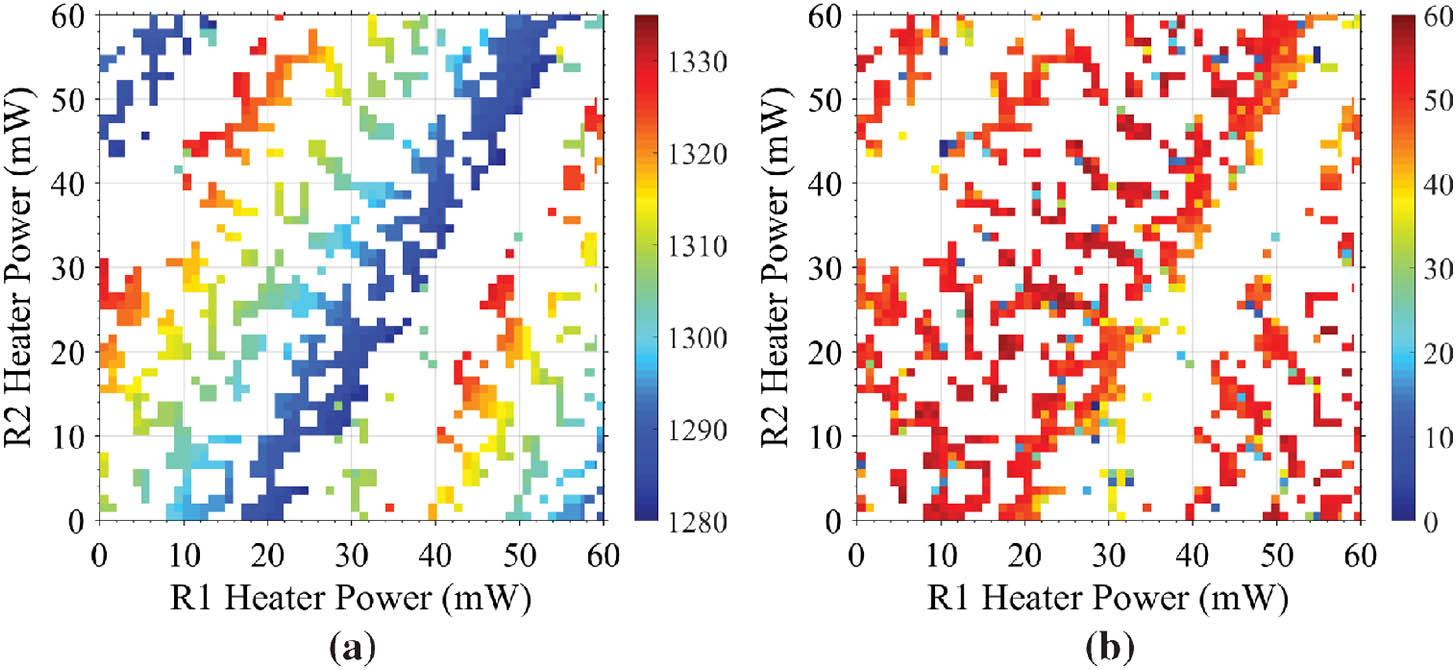
To evaluate the laser performance completely, all of the tuning elements in the laser cavity need to be optimized. This was achieved by applying electrical power to the heaters on both rings sequentially in steps of 1 mW (while the gain current was kept at a constant value of 300 mA). For each point, the phase section was tuned from 0 to 60 mW in 1 mW steps while monitoring the APD current. These power values were necessary to achieve a full 2π phase shift with some margin. The phase section was then set to maximize the APD photocurrent, and a spectral analysis was done using the wave meter to determine the number of lasing wavelengths quickly. A slower, high-resolution OSA scan was taken only for single-mode points. Obtaining the tuning map of the Vernier ring MZI laser is more complex than of the Vernier ring laser, as there are four tuning elements. The tuning algorithm was the same as that for the Vernier ring laser, except that both MZI and phase were sequentially tuned to maximize APD photocurrent. This tuning algorithm was executed using MATLAB scripts and Keithley SMU units. For more optimized tuning, a cycle of sequentially adjusting each heater should be iterated several times due to thermal cross-talk among the tuning elements. However, due to the large dimensional tuning space of the heaters (3D for two rings and phase and 4D with MZI) and also the limited speed of GPIB protocols, only one cycle was used for each data point. Tuning all the thermal phase tuners together can maintain a mode-hop-free operation in a short wavelength range dependent on the performance of the thermal phase shifter. The tuning map and SMSR are shown in Figs. 5(a) and 5(b), respectively, for the Vernier ring MZI laser. Figure 6(a) shows the spectra (after normalizing the grating coupler response) of the Vernier ring laser in the entire tuning range; Fig. 6(a) shows a single OSA trace with 52 dB SMSR, optimized manually with several iterations of heater adjustments to maximize both APD current and SMSR.
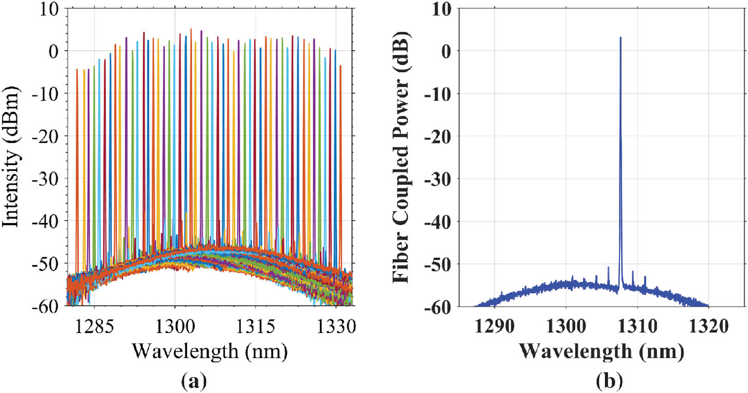
Fig. 5. Tuning map of the Vernier ring laser showing (a) peak wavelength and (b) SMSR.

下载图片 查看所有图片

Fig. 6. Vernier ring laser: (a) automatically measured spectra over the entire tuning range and (b) manually optimized spectrum at a single point showing 52 dB SMSR.

下载图片 查看所有图片

For the Vernier ring MZI laser, the tuning range increases to 53 nm, and the overall SMSR also improves as compared with the Vernier ring laser, which is a direct result of the additional wavelength filtering provided by the MZI. The corresponding spectra after normalizing the grating coupler response is shown in Fig. 7(a). A single OSA trace is shown in Fig. 7(b) with 58 dB SMSR, which is higher than that of the Vernier ring laser.
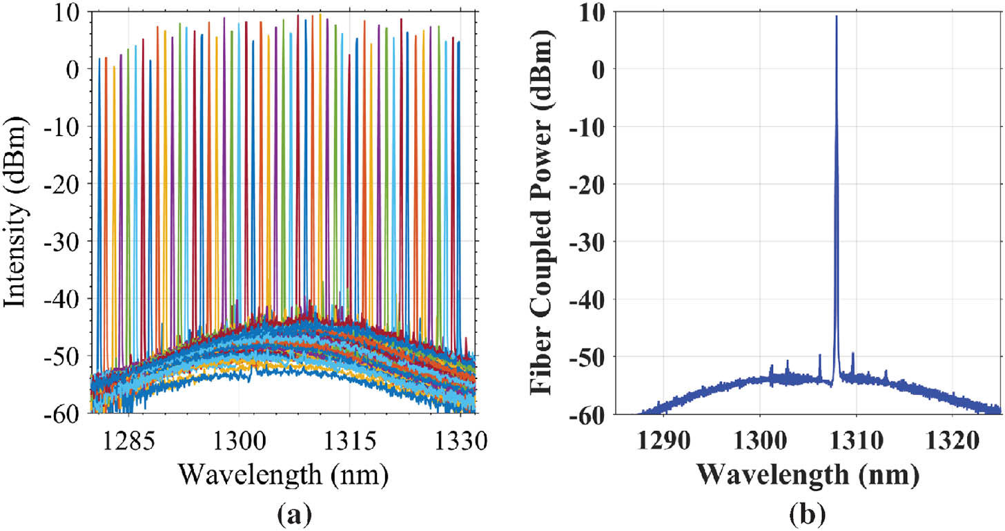
Fig. 7. Vernier ring MZI laser: (a) automatically measured spectra over the entire tuning range and (b) manually optimized spectrum at a single point showing 58 dB SMSR.

下载图片 查看所有图片

The measured tuning range and the SMSR for both devices decrease because of the gap reduction between the waveguide and the ring. With the correct design, the tuning range should increase to 70 nm for the Vernier ring MZI laser. Additionally, the gap reduction would increase the ring-bus coupling strength and, therefore, decrease the SMSR and increase the linewidth.

3.4 C. Spectral Linewidth

Linewidth enhancement in semiconductor lasers is a direct effect of coupling between the real and imaginary parts of the refractive index. This happens because any change in carrier density changes both material gain and the real part of refractive index. As a result, the effective linewidth is broadened from the predicted Schawlow–Townes linewidth. The linewidth for semiconductor lasers then becomes where ΔνST is the modified Schawlow–Townes linewidth. The low loss passive cavity is beneficial in reducing the spectral linewidth of the laser. A detailed description on linewidth narrowing in heterogeneously integrated lasers is provided in Ref. [31]. Under external feedback, the linewidth of a laser is modified to where F is the linewidth reduction factor and defined as The factors A and B are defined as where τ0 is the photon round-trip time in the active region, ϕeff is the effective phase of the external cavity, and reff is the effective reflectivity of the passive section. The factor A is proportional to the effective cavity length, which is increased by the photon re-circulation inside the ring resonators in the cavity. Since the volume of the active layer remains the same (fixed by the gain section length), the photons occupy a much larger volume when the effective cavity length increases thus reducing the net confinement factor. The decrease in confinement factor reduces the noise associated with spontaneous emission thus narrowing the linewidth. On the other hand, the factor B is associated with optical negative feedback, which narrows the linewidth when lasing is red-detuned from the resonance of the mirror’s reflectivity.

To qualitatively understand the linewidth narrowing in Vernier ring lasers, we show in Fig. 8(a) the numerically calculated magnitudes of coefficients A, B, and F for the designed Vernier ring mirror as a function of wavelength detuning from the mirror’s resonance peak. While the factor A is maximized at resonance peak (no detuning), the optimal detuning for greatest linewidth narrowing effect (factor F) occurs when the lasing wavelength is slightly longer than the resonance wavelength where factor B is maximized. In practice, however, it is much easier to tune the phase section to obtain lasing at the resonance peak by maximizing the laser output power. Figure 8(b) shows the estimated Lorentzian linewidth of our Vernier ring laser (detuned and no-detuning cases) and the solitary laser (gain section only) as functions of the linewidth enhancement factor, where silicon waveguide loss is 5 dB/cm and ring coupling coefficient is 0.18. As we can see, the laser linewidth can be reduced by more than an order of magnitude compared with a solitary laser by employing the Vernier ring as an external cavity. Furthermore, lowering the linewidth enhancement factor from 10 to 1 would result in more than one order of magnitude reduction in linewidth. Also, for low values of αH, the difference in linewidth between the optimally detuned and not detuned Vernier ring laser decreases, as the negative optical feedback (B) is proportional to linewidth enhancement factor αH [see Eq. (4)]. For QW lasers, the factor αH is found to be in the range of 2–5 [32]. Due to their atom-like transitions, QD lasers show a reduction in αH. In fact, it is possible to achieve a net zero value of αH in QD lasers by reducing the variation in the QD size and carefully modulating the p-doping [16,33]. The measured value of αH for QD lasers similar to this work was found to be in the range of 1–2 [34], which brings the expected linewidth for our QD lasers to be well below the 10 kHz level.
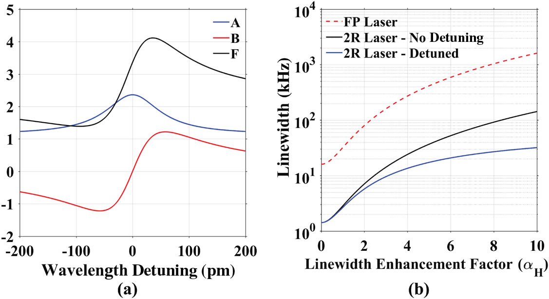
Fig. 8. (a) Coefficients A, B, F calculated for the Vernier ring laser cavity as functions of detuning from the ring resonance peak with αH=2. (b) Estimated Lorentzian linewidth as a function of linewidth enhancement factor. A waveguide loss of 5 dB/cm and an output power of 10 mW were used in the calculation.

下载图片 查看所有图片

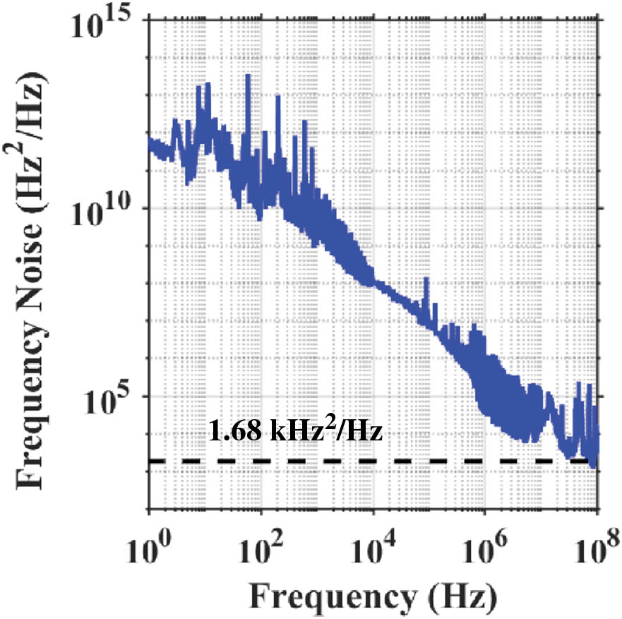
Experimental study of the negative optical feedback in our laser’s linewidth is, unfortunately, outside the scope of this work due to equipment limitations. Linewidth, therefore, was measured when the lasing is tuned to be right at the resonance peak by maximizing the photocurrent in the on-chip PD. The linewidth for both lasers was measured at various spectral points across the wavelength tuning range. The measured Lorentzian linewidth as a function of wavelength is shown in Figs. 9(a) and 9(b) for both laser types. For the Vernier ring laser, linewidth is within 10–20 kHz range except for some wavelengths near 1290 nm, where linewidth shoots up to 50 kHz. It is attributed to the poorer SMSR near the edge of the gain spectrum. With the inclusion of the MZI for better SMSR, the linewidth is consistently less than 10 kHz over the whole tuning range. Figure 10 shows the trace of frequency noise as a function of frequency for the best observed linewidth of the Vernier ring MZI laser. Several spikes can be seen in the plot, which are a result of the exposed probes. Appropriate packaging and shielding would remove these spikes. It is also worth pointing out that the white noise floor is not reached within the 100 MHz measurement range of the tool. A white noise upper-limit value of 1.68  kHz2/Hz is shown, which corresponds to a 5.3 kHz Lorentzian linewidth.
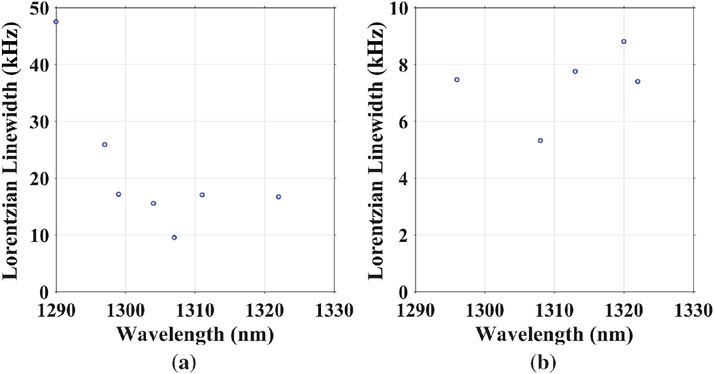
Fig. 9. Measured Lorentzian linewidth as a function of wavelength for (a) Vernier ring laser and (b) Vernier ring MZI laser.
下载图片 查看所有图片

Fig. 10. Measured frequency noise of the Vernier ring MZI laser in logarithmic scale over complete frequency range.

下载图片 查看所有图片

4. CONCLUSIONS

This paper reports design and measurement results of widely tunable heterogeneously integrated QD lasers on SOI waveguides operating in the O-band. We show a wide tuning range and the lowest linewidths reported in the literature for integrated lasers operating in the O-band. After adjusting for grating coupler loss, we have 10  dBm power in the silicon waveguide. Further improvements can be made to increase both the tuning range and reduce the linewidth by including three or four rings in the passive cavity [23,31] or using a combination of rings and Bragg gratings [35]. A low-loss silicon waveguide platform with extremely shallow etched waveguides can further reduce side-wall scattering loss in the passive cavity [36] and lower the linewidth significantly. The QD gain material can itself be changed to reduce the linewidth enhancement factor by techniques such as p-modulation doping. Even though these are the first demonstrations of heterogeneously integrated QD tunable lasers on silicon, the output power levels and the linewidth of our lasers are within the parameter range to be inserted in long-haul coherent communication networks.

5 Acknowledgment

Acknowledgment. The views and conclusions in this paper are those of the authors and should not be interpreted as presenting the official policies or positions, either expressed or implied, of DARPA, ARPA-E, or the U.S. government. The U.S. government is authorized to reproduce and distribute reprints for government purposes notwithstanding any copyright notation hereon.

References

[1] R. Jones, P. Doussiere, J. B. Driscoll, W. Lin, H. Yu, Y. Akulova, T. Komljenovic, J. E. Bowers. Heterogeneously integrated InP/silicon photonics: fabricating fully functional transceivers. IEEE Nanotechnol. Mag., 2019, 13: 17-26.

[2] LiehrM.BaierM.HoeflerG.FahrenkopfN. M.BowersJ.GladhillR.O’BrienP.TimurdoganE.SuZ.KishF., “Chapter 4–Foundry capabilities for photonic integrated circuits,” in Optical Fiber Telecommunications VII, WillnerA. E., ed. (Academic, 2020), pp. 143193.

[3] D. Bimberg, U. W. Pohl. Quantum dots: promises and accomplishments. Mater. Today, 2011, 14: 388-397.

[4] J. Duan, H. Huang, B. Dong, D. Jung, J. C. Norman, J. E. Bowers, F. Grillot. 1.3  μm reflection insensitive InAs/GaAs quantum dot lasers directly grown on silicon. IEEE Photon. Technol. Lett., 2019, 31: 345-348.

[5] S. Chen, W. Li, J. Wu, Q. Jiang, M. Tang, S. Shutts, S. N. Elliott, A. Sobiesierski, A. J. Seeds, I. Ross, P. M. Smowton, H. Liu. Electrically pumped continuous-wave III–V quantum dot lasers on silicon. Nat. Photonics, 2016, 10: 307-311.

[6] A. Y. Liu, J. Peters, X. Huang, D. Jung, J. Norman, M. L. Lee, A. C. Gossard, J. E. Bowers. Electrically pumped continuous-wave 1.3  μm quantum-dot lasers epitaxially grown on on-axis (001) GaP/Si. Opt. Lett., 2017, 42: 338-341.

[7] B. Tian, Z. Wang, M. Pantouvaki, P. Absil, J. Van Campenhout, C. Merckling, D. Van Thourhout. Room temperature O-band DFB laser array directly grown on (001) silicon. Nano Lett., 2017, 17: 559-564.

[8] J. C. Norman, D. Jung, Z. Zhang, Y. Wan, S. Liu, C. Shang, R. W. Herrick, W. W. Chow, A. C. Gossard, J. E. Bowers. A review of high-performance quantum dot lasers on silicon. IEEE J. Quantum Electron., 2019, 55: 2000511.

[9] D. Jung, Z. Zhang, J. Norman, R. Herrick, M. J. Kennedy, P. Patel, K. Turnlund, C. Jan, Y. Wan, A. C. Gossard, J. E. Bowers. Highly reliable low-threshold InAs quantum dot lasers on on-axis (001) Si with 87% injection efficiency. ACS Photon., 2018, 5: 1094-1100.

[10] Y. Han, Z. Yan, W. K. Ng, Y. Xue, K. S. Wong, K. M. Lau. Bufferless 1.5  μm III–V lasers grown on Si-photonics 220  nm silicon-on-insulator platforms. Optica, 2020, 7: 148-153.

[11] BowersJ. E.ChangL.HuangD.MalikA.NethertonA.TranM.XieW.XiangC., “Terabit transmitters using heterogeneous III–V/Si photonic integrated circuits,” in Optical Fiber Communication Conference (OFC) (Optical Society of America, 2020), paper W3F.1.

[12] D. J. Blumenthal, R. Heideman, D. Geuzebroek, A. Leinse, C. Roeloffzen. Silicon nitride in silicon photonics. Proc. IEEE, 2018, 106: 2209-2231.

[13] Y. Fan, A. van Rees, P. J. M. van der Slot, J. Mak, R. M. Oldenbeuving, M. Hoekman, D. Geskus, C. G. H. Roeloffzen, K.-J. Boller. Hybrid integrated InP-Si3N4 diode laser with a 40-Hz intrinsic linewidth. Opt. Express, 2020, 28: 21713-21728.

[14] C. Xiang, W. Jin, J. Guo, J. D. Peters, M. J. Kennedy, J. Selvidge, P. A. Morton, J. E. Bowers. Narrow-linewidth III–V/Si/Si3N4 laser using multilayer heterogeneous integration. Optica, 2020, 7: 20-21.

[15] T. Komljenovic, S. Srinivasan, E. Norberg, M. Davenport, G. Fish, J. E. Bowers. Widely tunable narrow-linewidth monolithically integrated external-cavity semiconductor lasers. IEEE J. Sel. Top. Quantum Electron., 2015, 21: 214-222.

[16] Y. Wang, S. Chen, Y. Yu, L. Zhou, L. Liu, C. Yang, M. Liao, M. Tang, Z. Liu, J. Wu, W. Li, I. Ross, A. J. Seeds, H. Liu, S. Yu. Monolithic quantum-dot distributed feedback laser array on silicon. Optica, 2018, 5: 528-533.

[17] Y. Wan, S. Zhang, J. C. Norman, M. J. Kennedy, W. He, S. Liu, C. Xiang, C. Shang, J.-J. He, A. C. Gossard, J. E. Bowers. Tunable quantum dot lasers grown directly on silicon. Optica, 2019, 6: 1394-1400.

[18] Y. Wan, S. Zhang, J. C. Norman, M. Kennedy, W. He, Y. Tong, C. Shang, J.-J. He, H. K. Tsang, A. C. Gossard, J. E. Bowers. Directly modulated single-mode tunable quantum dot lasers at 1.3  μm. Laser Photon. Rev., 2020, 14: 1900348.

[19] S. Uvin, S. Kumari, A. D. Groote, S. Verstuyft, G. Lepage, P. Verheyen, J. V. Campenhout, G. Morthier, D. V. Thourhout, G. Roelkens. 1.3  μm InAs/GaAs quantum dot DFB laser integrated on a Si waveguide circuit by means of adhesive die-to-wafer bonding. Opt. Express, 2018, 26: 18302-18309.

[20] SuG.-L.SakibM. N.HeckJ.RongH.WuM. C., “A heterogeneously-integrated III–V/silicon interferometric widely tunable laser,” in OSA Advanced Photonics Congress (AP) 2019 (IPR, Networks, NOMA, SPPCom, PVLED) (Optical Society of America, 2019), paper IW3A.1.

[21] H. Duprez, C. Jany, C. Seassal, B. B. Bakir. Highly tunable heterogeneously integrated III–V on silicon sampled-grating distributed Bragg reflector lasers operating in the O-band. Opt. Express, 2016, 24: 20895-20903.

[22] Z. Zhang, D. Jung, J. C. Norman, W. W. Chow, J. E. Bowers. Linewidth enhancement factor in InAs/GaAs quantum dot lasers and its implication in isolator-free and narrow linewidth applications. IEEE J. Sel. Top. Quantum Electron., 2019, 25: 1900509.

[23] M. A. Tran, D. Huang, J. Guo, T. Komljenovic, P. A. Morton, J. E. Bowers. Ring-resonator based widely-tunable narrow-linewidth Si/InP integrated lasers. IEEE J. Sel. Top. Quantum Electron., 2020, 26: 1500514.

[24] R. Wang, A. Malik, I. Šimonytė, A. Vizbaras, K. Vizbaras, G. Roelkens. Compact GaSb/silicon-on-insulator 2.0  μm widely tunable external cavity lasers. Opt. Express, 2016, 24: 28977-28986.

[25] B. Tossoun, G. Kurczveil, C. Zhang, A. Descos, Z. Huang, A. Beling, J. C. Campbell, D. Liang, R. G. Beausoleil. Indium arsenide quantum dot waveguide photodiodes heterogeneously integrated on silicon. Optica, 2019, 6: 1277-1281.

[26] DavenportM. L.TranM. A.KomljenovicT.BowersJ. E., “Chapter six–Heterogeneous integration of III–V lasers on Si by bonding,” in Silicon Photonics, LourdudossS.ChenR. T.JagadishC., eds., vol. 99 of Semiconductors and Semimetals (Elsevier, 2018), pp. 139188.

[27] G. Kurczveil, D. Liang, M. Fiorentino, R. G. Beausoleil. Robust hybrid quantum dot laser for integrated silicon photonics. Opt. Express, 2016, 24: 16167-16174.

[28] B. J. Stevens, D. T. D. Childs, H. Shahid, R. A. Hogg. Direct modulation of excited state quantum dot lasers. Appl. Phys. Lett., 2009, 95: 061101.

[29] E. U. Rafailov, A. D. McRobbie, M. A. Cataluna, L. O’Faolain, W. Sibbett, D. A. Livshits. Investigation of transition dynamics in a quantum-dot laser optically pumped by femtosecond pulses. Appl. Phys. Lett., 2006, 88: 041101.

[30] M. A. Cataluna, W. Sibbett, D. A. Livshits, J. Weimert, A. R. Kovsh, E. U. Rafailov. Stable mode locking via ground- or excited-state transitions in a two-section quantum-dot laser. Appl. Phys. Lett., 2006, 89: 081124.

[31] M. A. Tran, D. Huang, J. E. Bowers. Tutorial on narrow linewidth tunable semiconductor lasers using Si/III–V heterogeneous integration. APL Photon., 2019, 4: 111101.

[32] M. Osinski, J. Buus. Linewidth broadening factor in semiconductor lasers-an overview. IEEE J. Quantum Electron., 1987, 23: 9-29.

[33] W. W. Chow, Z. Zhang, J. C. Norman, S. Liu, J. E. Bowers. On quantum-dot lasing at gain peak with linewidth enhancement factor αH = 0. APL Photon., 2020, 5: 026101.

[34] B. Dong, H. Huang, J. Duan, G. Kurczveil, D. Liang, R. G. Beausoleil, F. Grillot. Frequency comb dynamics of a 1.3 μm hybrid-silicon quantum dot semiconductor laser with optical injection. Opt. Lett., 2019, 44: 5755-5758.

[35] D. Huang, M. A. Tran, J. Guo, J. Peters, T. Komljenovic, A. Malik, P. A. Morton, J. E. Bowers. High-power sub-kHz linewidth lasers fully integrated on silicon. Optica, 2019, 6: 745-752.

[36] M. Tran, D. Huang, T. Komljenovic, J. Peters, A. Malik, J. Bowers. Ultra-low-loss silicon waveguides for heterogeneously integrated silicon/III-V photonics. Appl. Sci., 2018, 8: 1139.

Aditya Malik, Joel Guo, Minh A. Tran, Geza Kurczveil, Di Liang, John E. Bowers. Widely tunable, heterogeneously integrated quantum-dot O-band lasers on silicon[J]. Photonics Research, 2020, 8(10): 10001551.
引用该论文: TXT   |   EndNote

相关论文

加载中...

关于本站 Cookie 的使用提示

中国光学期刊网使用基于 cookie 的技术来更好地为您提供各项服务,点击此处了解我们的隐私策略。 如您需继续使用本网站,请您授权我们使用本地 cookie 来保存部分信息。
全站搜索
您最值得信赖的光电行业旗舰网络服务平台!