Chinese Optics Letters, 2019, 17 (7): 072301, Published Online: Jul. 9, 2019   

All-optical logic gates and a half-adder based on lithium niobate photonic crystal micro-cavities Download: 2686次

Author Affiliations
State Key Laboratory of Advanced Optical Communication Systems and Networks, School of Physics and Astronomy, Shanghai Jiao Tong University, Shanghai 200240, China
Abstract
All-optical logic gates including AND, XOR, and NOT gates, as well as a half-adder, are realized based on two-dimensional lithium niobate photonic crystal (PhC) circuits with PhC micro-cavities. The proposed all-optical devices have an extinction ratio as high as 23 dB due to the effective all-optical switch function induced by two-missing-hole micro-cavities. These proposed devices can have potential implementation of complex integrated optical functionalities including all-optical computing in a lithium niobate slab or thin film.

Current all-optical logic gates are predominantly fabricated in optical fiber waveguides, which make it difficult to integrate on small integrated chips[1,2], whereas defect waveguides in photonic crystals (PhCs) possess small scale and unique light controlling ability[3] that make it a crucial method to design miniaturized all-optical logic gates. Until now, all-optical logic gates are mostly designed and integrated on silicon-based PhC materials[4,5]. However the two-photon absorption and third-order nonlinearity in silicon may cause nonlinear loss and signal crosstalk, which results in low extinction ratio in silicon logic gates. Consequently, a new optical material integration platform is demanded, such as lithium niobate (LiNbO3, LN), which attracts more research interests where second-order nonlinearity is dominated. LN also possesses unique electro-optic, acousto-optic, piezoelectric, and other physical properties[69" target="_self" style="display: inline;">9]. So, LN and LN thin film (LNOI)[1014" target="_self" style="display: inline;">14] could be the ideal materials for the development of the integrated optical circuits. Based on the above photonics platform, developing all-optical logic gates is significant in integrated photonics computing.

We have experimentally demonstrated polarization-based binary optical logic gates by employing the Pockels effect in periodically poled LN in our previous research works[15,16], where we only get an extinction ratio of about 10 dB. In this Letter, we have designed three basic all-optical logic gates with 23 dB, including AND, XOR, and NOT gates in an LN PhC by employing PhC micro-cavities. We have found that the extinction ratio between the logic 1 and 0 states can be improved by adding PhC-defect micro-cavities in the PhC circuits[17,18]. By utilizing the single-line-defect (W1) waveguides and two-missing-hole (L2) cavities, the extinction ratio of the logic gates we designed can reach a maximum as high as 23 dB in the finite-difference time-domain (FDTD) simulations (the simulated software used is RSOFT). It is the highest extinction ratio obtained, to the best of our knowledge, compared with 20.53 dB in silicon PhC[4]. Finally, an all-optical half-adder was also designed and realized effectively by the combination of these basic logic gates in an LN PhC.

Figure 1(a) shows the band diagrams and square lattice sketch of a two-dimensional square lattice PhC with 5% MgO-doped LN rods, where r is the radius of the rods, and a is the lattice constant, respectively. The duty ratio is set as r/a=0.26, and the refractive index of 5% MgO-doped LN rods was calculated by employing the Sellmeier equation at the 1.55 μm wavelength[19]. The band diagrams of this lattice structure are simulated by the plane wave expansion method (PWE). It shows that this lattice structure has large transverse electric (TE) mode band gap ranging from 0.38 (a/λ) to 0.43 (a/λ). Under the condition of the 1.55 μm C-band window with a corresponding 0.40 (a/λ) band gap, the lattice constant of the PhC can be calculated as 0.620 μm.

Fig. 1. (a) Band diagrams in a square lattice PhC with LN (MgO-doped) rods for TE and TM modes. (b) The left is the schematic structure of the W1 waveguide in the Γ-M direction; the right is the FDTD simulation result of the W1 waveguide and the sketch of the light beam coherent interference.

下载图片 查看所有图片

The light cannot propagate in the PhC forbidden band. However, the defect waveguides called W1 waveguides[20] in the PhC possess unique light guiding ability due to the existence of the band gap. So the W1 waveguide is designed as the basic element of the all-optical logic gates in LN PhC structures. The PhC line-defect waveguide is fabricated by removing the line rods, as shown in the left of Fig. 1(b). According to the wave optics theory, if the phase difference between the two light beams that are incident from input A and input B is 2kπ (where k=0,1,2,), then constructive interference can occur, and the output light will have high power (corresponding to logic state 1 as the output C performance)[21]. On the contrary, destructive interference can occur when the phase difference is (2k+1)π (where k=0,1,2,), and the output light will be approximately zero (corresponding to logic state 0 as the output D performance).

The W1 waveguide can guide the light in the PhC structure, and besides, the point-defect micro-cavities located next to the line-defect waveguides in PhC can effectively affect the transmission of the light beams. There are several different micro-cavities in the PhC, one of which is the other basic element called the L2 cavity formed by getting rid of two adjacent rods[20]. Figure 2 demonstrates the all-optical switch function of the L2 cavity. The T-shape W1 waveguide without the L2 cavity in Fig. 2(a) has the same relative output intensity, which approximately equals 0.3 in the two opposite output ports, A and B. When the L2 cavity is located near the output B port, the relative output intensity in output B is reduced to 0.2. Due to the light coupling effect of the L2 cavity, the relative output intensity in output A can be enhanced to 0.4, as shown in Fig. 2(b). The modulation results demonstrate that the L2 cavity can assist the W1 waveguide to realize the desired splitting ratio of the light beams.

Fig. 2. T-shape W1 waveguides (a) without or (b) with the L2 cavity in an LN PhC and the FDTD simulated different transmission results.

下载图片 查看所有图片

Here, we proposed a complicated LN PhC structure to realize three basic all-optical logic gates and a half-adder with a high extinction ratio by combining the W1 waveguides with L2 cavities. Figure 3 shows the schematic structures of the three fundamental all-optical logic gates. First, the AND gate is composed of two L2 cavities located next to the input A and input B ports, as shown in Fig. 3(a), and the output C port is placed at the position where constructive interference can occur. When the two L2 cavities are located next to the output C port, this structure can form the XOR gate, as illustrated by Fig. 3(b), while the NOT gate is realized by replacing the input B port by the control port whose logic state is always set as 1 on the basis of XOR gate, as shown in Fig. 3(c). The truth table for the AND, XOR, and NOT logic gates is shown in Table 1.

Table 1. Truth Table for the AND, XOR, and NOT Logic Gates

Input AInput BANDXORNOT
0000\
01011
1001\
11100

查看所有表

Fig. 3. Three all optical logic gates (a) AND, (b) XOR, and (c) NOT in an LN PhC with different micro-cavities locations.

下载图片 查看所有图片

Figure 4 shows the FDTD simulated transmission of the AND and XOR gates in an LN PhC. The input logic state 1 corresponds to the input light value over 0.5, as the black dotted line. Output logic state 1 corresponds to the value higher than 0.6 when input A=1 and B=1, while output logic state 0 corresponds to the value lower than 0.2 when input A=1 and B=0. The extinction ratio of the XOR gate in Fig. 4(b) between the logic states 1 and 0 is as high as 23 dB.

Fig. 4. FDTD simulated transmission of (a) AND and (b) XOR gates in an LN PhC.

下载图片 查看所有图片

In Fig. 4(b), the output C port is placed at the position where the destructive interference occurs. When input A=1 and B=1, the C port has no light coming out because of the destructive interference effect. In this XOR gate, the L2 cavities are placed next to the output C port. Therefore, when the input light comes from either side of A or B, it can be coupled into the L2 cavity, which will strengthen the light intensity coming out of output C. The L2 cavity was chosen after a comparison with the L3 cavity in this Letter. For the AND gate, the L3 cavity has decreased the extinction ratio, and the XOR gate cannot work as usual.

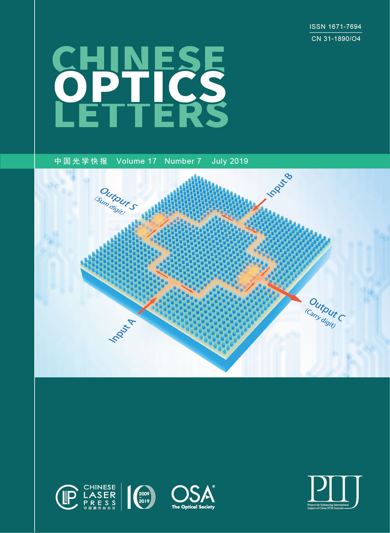
Then, we designed an all-optical half-adder by the combination of the AND and XOR gates, as shown in Fig. 5(a). Table 2 shows the truth table for the all-optical half-adder. The sum digit of the half-adder is the XOR gate, and the carry digit corresponds to the AND gate. Figure 5(b) shows the FDTD simulated transmission of the all-optical half-adder in an LN PhC. The simulation results show that this all-optical half-adder can implement good basic logic functions.

Table 2. Truth Table for the All-optical Half-adder

Input AInput BOutput C (Carry Digit)Output S (Sum Digit)
0000
0101
1001
1110

查看所有表

Fig. 5. (a) Schematic structure of the all-optical half-adder in an LN PhC. (b) The FDTD simulated transmission of the all-optical half-adder.

下载图片 查看所有图片

In conclusion, assisted by different micro-cavities in LN PhC circuits, we have achieved the AND, XOR, and NOT logic gates and an all-optical half-adder in an LN PhC, which has the highest extinction ratio of 23 dB compared with that in silicon logic gates[4,5]. This logic gate design may benefit complex integrated all-optical functionalities in the LN or LNOI photonics device platform, such as optical quantum computing by combining parametric down-conversion nonlinear processes[22].

References

[1] HuoL.LinC.ChanC.-K.ChenL.-K., in Optical Fiber Communication Conference (Optical Society of America, 2007), paper OThI4.

[2] BogoniA.PotiL.ProiettiR.MeloniG.PonziniF.GhelfiP., Electron. Lett.41, 435 (2005).ELLEAK0013-5194

[3] MekisA.ChenJ.KurlandI.FanS.VilleneuveP. R.JoannopoulosJ., Phys. Rev. Lett.77, 3787 (1996).PRLTAO0031-9007

[4] Mohebzadeh-BahabadyA.OlyaeeS., IET Optoelectron.12, 191 (2018).

[5] RaniP.KalraY.SinhaR. K., Opt. Commun.298, 227 (2013).OPCOB80030-4018

[6] SohlerW.HuH.RickenR.QuiringV.VannahmeC.HerrmannH.BüchterD.RezaS.GrundkötterW.OrlovS.SucheH.NourooziR.MinY., Opt. Photon. News19, 24 (2008).OPPHEL1047-6938

[7] WongK.-K., Properties of Lithium Niobate (IET, 2002).

[8] MaB.KafkaK.ChowdhuryE., Chin. Opt. Lett.15, 5 (2017).CJOEE31671-7694

[9] ZhuC.ChenY.LiG.GeL.ZhuB.HuM.ChenX., Chin. Opt. Lett.15, 091901 (2017).CJOEE31671-7694

[10] WangC.ZhangM.ChenX.BertrandM.Shams-AnsariA.ChandrasekharS.WinzerP.LončarM., Nature562, 101 (2018).

[11] GeL.ChenY.JiangH.LiG.ZhuB.LiuY.ChenX., Photon. Res.6, 954 (2018).

[12] JiangH.LiangH.LuoR.ChenX.ChenY.LinQ., Appl. Phys. Lett.113, 021104 (2018).APPLAB0003-6951

[13] BoesA.CorcoranB.ChangL.BowersJ.MitchellA., Laser Photon. Rev.12, 1700256 (2018).

[14] WangL.WangC.WangJ.BoF.ZhangM.GongQ.LončarM.XiaoY. F., Opt. Lett.43, 2917 (2018).OPLEDP0146-9592

[15] ZhangY.ChenY.ChenX., Appl. Phys. Lett.99, 161117 (2011).APPLAB0003-6951

[16] JiangH.ChenY.LiG.ZhuC.ChenX., Opt. Express23, 9784 (2015).OPEXFF1094-4087

[17] AkahaneY.MochizukiM.AsanoT.TanakaY.NodaS., Appl. Phys. Lett.82, 1341 (2003).APPLAB0003-6951

[18] KuramochiE.SmithD. H.NozakiK.ShinyaA.NotomiM., in Conference on Lasers and Electro-Optics (CLEO) (IEEE, 2016), p. 1.

[19] ZelmonD. E.SmallD. L.JundtD., J. Opt. Soc. Am.14, 3319 (1997).

[20] TalneauA.LalanneP.AgioM.SoukoulisC. M., Opt. Lett.27, 1522 (2002).OPLEDP0146-9592

[21] AndalibP.GranpayehN., J. Opt. Soc. Am.26, 10 (2009).

[22] LengH.YuX.GongY.XuP.XieZ.JinH.ZhangC.ZhuS., Nat. Commun.2, 429 (2011).NCAOBW2041-1723

Chenghao Lu, Bing Zhu, Chuanyi Zhu, Licheng Ge, Yian Liu, Yuping Chen, Xianfeng Chen. All-optical logic gates and a half-adder based on lithium niobate photonic crystal micro-cavities[J]. Chinese Optics Letters, 2019, 17(7): 072301.

本文已被 3 篇论文引用
被引统计数据来源于中国光学期刊网
引用该论文: TXT   |   EndNote

相关论文

加载中...

关于本站 Cookie 的使用提示

中国光学期刊网使用基于 cookie 的技术来更好地为您提供各项服务,点击此处了解我们的隐私策略。 如您需继续使用本网站,请您授权我们使用本地 cookie 来保存部分信息。
全站搜索
您最值得信赖的光电行业旗舰网络服务平台!