Research progress in large-area perovskite solar cells  Download: 913次
1 Key Laboratory of Semiconductor Materials Science, Institute of Semiconductors, Chinese Academy of Sciences, Beijing 100083, China
2 College of Materials Science and Opto-electronic Technology, University of Chinese Academy of Sciences, Beijing 100049, China
Figures & Tables
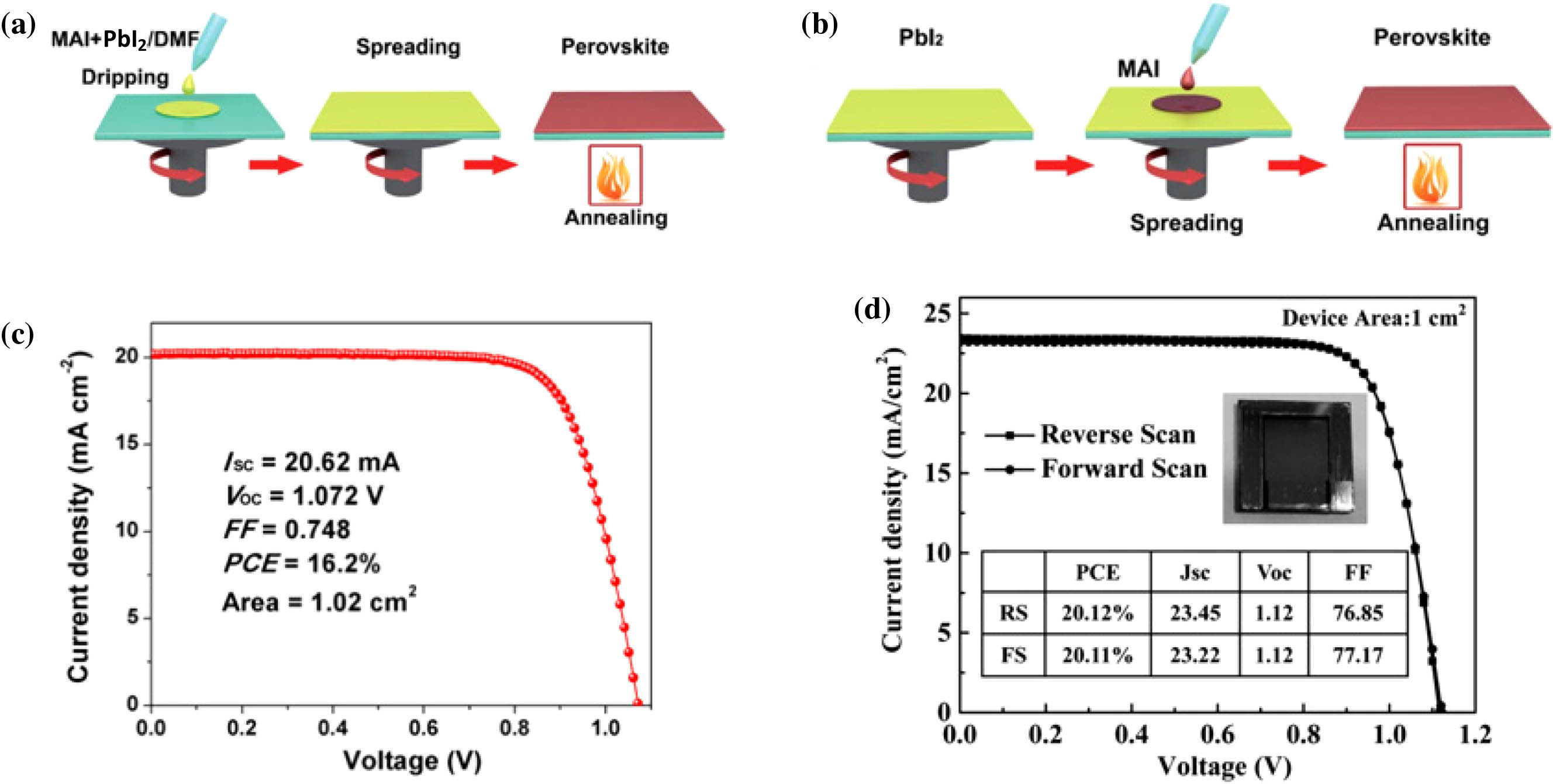
Fig. 1. (a) One-step deposited perovskite films. (b) Two-step deposited perovskite films. (c) J-V curve of the best large cell endowed with anti-reflection film. (d) J-V curve of the PSCs in large size of 1 cm2 measured under reverse and forward scan under one-sun condition. (a), (b) Reproduced with permission [26], Copyright 2018, Royal Society of Chemistry. (c) Reproduced with permission [17], Copyright 2015, American Association for the Advancement Science. (d) Reproduced with permission [19], Copyright 2017, Nature Publishing Group.
下载图片 查看原文
Fig. 2. (a) Schematic illustration for the blade coating of perovskite film in the Landau–Levich mode. (b) The perovskite film’s thickness as a function of blade-coating speed by coating a 1 mol/L MAPbI3/DMF solution on a 145°C preheated substrate. (c) Schematic illustration for N2-knife-assisted blade coating of perovskite films. (d) Schematic illustration showing the drying of ink into a perovskite/intermediate film and full crystallization of a perovskite film. VNCS, volatile noncoordinating solvent; NVCS, nonvolatile coordinating solvent. (a) Reproduced with permission [21], Copyright 2018, Nature Publishing Group. (b)–(d) Reproduced with permission [29], Copyright 2019, American Association for the Advancement Science.
下载图片 查看原文
Fig. 3. (a) Schematic illustration of the key steps involved in slot-die coating of perovskite thin films. (b) and (c) Schematic drawing of a module and J-V curve of an organometal halide perovskite solar cell, respectively. (d) The slot-die coating process for preparing CH3NH3PbI3 films. (e) and (f) 15.24 cm × 15.24 cm perovskite module and I-V curve, respectively. (a) Reproduced with permission [30], Copyright 2018, Royal Society of Chemistry. (b) and (c) Reproduced with permission [31], Copyright 2014, Wiley. (d) Reproduced with permission [33], Copyright 2018, Elsevier. (e) and (f) Reproduced with permission [34], Copyright 2018, Elsevier.
下载图片 查看原文
Fig. 4. (a) Schematic of concurrently pumped ultrasonic spray coating for perovskite precursor deposition. (b) A spray-coated four-cell module (3.8 cm2) from the 75% (molar fraction) PbAc2 with PbCl2. (c) and (d) Schematic representation of the megasonic spray-coating process and J-V curves of perovskite solar cells, respectively. (a) and (b) Reproduced with permission [35], Copyright 2016, Royal Society of Chemistry. (c) and (d) Reproduced with permission [38], Copyright 2018, Wiley.
下载图片 查看原文
Fig. 5. Schematic diagrams for the two main inkjet-printing methods: (a) continuous inkjet printing (CIJ); (b) drop-on-demand (DOD) inkjet printing. (c) 10 cm×10 cm device and (d) 10 cm×5 cm device. (e) Schematic illustration of PSC fabrication through inkjet printing with vacuum annealing. (f) J–V curves of PSCs on inkjet printing with active area 2.02 cm2. (a) and (b) Reproduced with permission [40], Copyright 2019, Wiley. (c) and (d) Reproduced with permission [41], Copyright 2016, Royal Society of Chemistry. (e) Reproduced with permission [42], Copyright 2018, Wiley. (f) Reproduced with permission [43], Copyright 2018, Elsevier.
下载图片 查看原文
Fig. 6. (a)–(c) Roll-to-roll processing setup for continuous preparation of perovskite solar cells. (a) Reproduced with permission [34], Copyright 2018, Elsevier. (b) Reproduced with permission [44], Copyright 2019, Wiley. (c) Reproduced with permission [45], Copyright 2019, Wiley.
下载图片 查看原文
Fig. 7. (a) Schematic illustration of vacuum-flash-assisted solution processing (VASP). (b) Surface scanning electron microscope (SEM) images of the perovskite films fabricated by the conventional process and vacuum-assisted solution process. (c) Diagram of the pressure-processing method for the deposition of perovskite films. (d) Surface SEM images of the perovskite films fabricated by the pressure-processing method and spin coating. (a) and (b) Reproduced with permission [20], Copyright 2015, Royal Society of Chemistry. (c) and (d) Reproduced with permission [46], Copyright 2016, American Association for the Advancement of Science.
下载图片 查看原文
Fig. 8. Evolution of the best reported lab-cell (≤0.1 cm2) efficiencies and large-area (≥1.0 cm2) device efficiencies. Reproduced with permission [47], Copyright 2018, American Association for the Advancement of Science.
下载图片 查看原文
Fig. 9. SEM images of (a) surfaces and (b) cross-sections of perovskite films prepared with different solvents, respectively. Reproduced with permission [29], Copyright 2018, American Association for the Advancement of Science.
下载图片 查看原文
Fig. 10. (a) Morphological characterization of perovskite MAPbI3 films with different amounts of Cl− incorporation by optical microscopy (top row), SEM (middle row), and atomic force microscope (AFM) (bottom row). (b) Top-view SEM images of perovskite films prepared with different excess amounts of MACl using blade-coating (top row) and spin-coating (bottom row) methods. (c) Photograph of the 1.1 μm thick MAPbI3 (Cl) film on a 5 cm×5 cm substrate, 12.0 cm2 six-cell perovskite solar module, and J–V curve of the 5 cm×5 cm perovskite module with an active area of 12.0 cm2. (d) Schematic illustration of perovskite film nucleation/crystallization from solvent bathing. (a) Reproduced with permission [51], Copyright 2016, Wiley. (b) Reproduced with permission [52], Copyright 2017, Nature Publishing Group. (c) Reproduced with permission [53], Copyright 2018, Nature Publishing Group. (d) Reproduced with permission [54], Copyright 2015, Wiley.
下载图片 查看原文
Fig. 11. (a)–(d) Top-view SEM images of perovskite films made with different amounts PbCl2 in the mixed lead source. (e) The crystal grain size and pinhole area in the perovskite films as a function of PbCl2 fraction. (f) XRD patterns and UV-Vis spectra, and (g)–(i) SEM images of FAMA/CsFAMA/KCsFAMA perovskite films, respectively. (j) Optical image of a 10 cm×10 cm HCVD Cs0.1FA0.9PbI2.9Br0.1-based solar module. (k) J-V curve of the champion solar module (14 subcells in series). (a)–(e) Reproduced with permission [55], Copyright 2016, Royal Society of Chemistry. (f)–(i) Reproduced with permission [56], Copyright 2017, Royal Society of Chemistry. (j) and (k) Reproduced with permission [57], Copyright 2019, Royal Society of Chemistry.
下载图片 查看原文
Fig. 12. (a) Scheme of the cell configuration highlighting the doped charge carrier extraction layers. (b) J–V curve of the best large cell endowed with antireflection film. (c) Comparison of the Bifluo-OMeTAD molecule (upper) and Spiro-OMeTAD (Merck) molecule. (d) J-V curve of PSCs with HTLs Bifluo-OMeTAD and Spiro-OMeTAD. (e) The structure of using P3HT as the HTL and structure of the interface between the P3HT and WBH. (f) I-V curves of solar modules formed by depositing the P3HT layer using bar-coating (purple) and spin-coating (orange) methods. (g) The DFT simulation of GO and Cl-GO. (h) PL spectra and TRPL spectra for different films. (a) and (b) Reproduced with permission [19], Copyright 2017, Wiley. (c) and (d) Reproduced with permission [74], Copyright 2017, Nature Publishing Group. (e) and (f) Reproduced with permission [75], Copyright 2019, Nature Publishing Group. (g) and (h) Reproduced with permission [76], Copyright 2019, American Association for the Advancement of Science.

下载图片 查看原文
Table1. Photovoltaic Performance of Perovskite Solar Cells Prepared by Different Methods
| Deposition Method | Device Structure | Device Area () | PCE (%) | Jsc () | Voc (V) | FF (%) | Reference | | Spin coating | | 1.02 | 16.2 | 20.21 | 1.072 | 74.8 | [17] | | Spin coating | | 1 | 20.12 | 23.45 | 1.12 | 76.85 | [19] | | Blade coating | | — | 10.44 | 16.73 | 0.96 | 65.0 | [28] | | Blade coating | | 33.0 | 15.0 | 19.5 | 1.07 | 72.1 | [21] | | 57.2 | 15.0 | 20.3 | 1.07 | 68.9 | | Blade coating | | 63.7 | 16.9 | 74.5 (mA) | 18.9 | 76.2 | [21] | | Slot-die coating | | 30 | 14.47 | 3.3 | 6.54 | 67.0 | [16] | | Slot-die coating | | 1 | 18.0 | 21.5 | 1.10 | 76.0 | [30] | | Slot-die coating | | 0.1 | 11.6 | 19.35 | 0.96 | 63.0 | [31] | | 47.3 | 4.57 | — | — | — | | Slot-die coating | | 0.1 | 11.96 | 20.38 | 0.98 | 60.0 | [32] | | Slot-die coating | | 0.1 | 15.75 | 19.79 | 1.02 | 77.15 | [33] | | Slot-die coating | | 168.75 | 11.1 | 0.69 | 21.2 | 68.0 | [34] | | 149.5 | 11.8 | 0.76 | 20.8 | 71.0 | | Spray coating | | 0.025 | 11.1 | 16.8 | 0.92 | 72.0 | [36] | | Spray coating | | 40 | 15.5 | 84.1 (mA) | 10.5 | 70.16 | [37] | | Spray coating | | 3.8 | 11.7 | 19.4 | 3.31 | 70.0 | [35] | | Spray coating | | 1 | 14.2 | 21.3 | 1.03 | 65.0 | [38] | | Inkjet printing | (drop casted perovskite through carbon layer) | 31 | 10.46 | 19.6 | 3.72 | 57.5 | [41] | | 70 | 10.75 | 17.72 | 9.63 | 62.9 | | Inkjet printing | | 4 | 13.24 | 20.4 | 1.04 | 62.57 | [42] | | Inkjet printing | | 2.02 | 17.74 | 21.88 | 1.06 | 76.5 | [43] | | Roll-to-roll | | 6.25 | 11.16 | 17.39 | 0.99 | 64.82 | [34] | | Vacuum-flash-assisted solution process | | 1 | 20.38 | 23.19 | 1.143 | 76.0 | [46] | | Pressure-processing method | | 36.1 | 15.7 | 71.1 | 10.5 | 75.7 | [22] |
|
查看原文
Table2. Photovoltaic Performance of Perovskite Solar Cells Prepared by Using Different Materials as Additives for Perovskite Layers
| Materials | Perovskite Components | Device Area () | PCE (%) | Jsc () | Voc (V) | FF (%) | Reference | | DMSO | | 1 | 20.12 | 23.45 | 1.12 | 76.85 | [19] | | Nonvolatile coordinating solvents (2-methoxyethanol and acetonitrile) | | 63.7 | 16.9 | 18.9 | 74.5 | 76.2 | [29] | | MACl, | | 1 | 15.4 | 21.0 | 1.06 | 69.1 | [51] | | 25 | 12.0 | 2.6 | 0.798 | 58.2 | | MACl | | 1.2 | 17.33 | 21.38 | 1.11 | 72.9 | [52] | | MACl | | 25 | 15.3 | 3.66 | 6.65 | 63.0 | [53] | | MAI | | 1.2 | 15.3 | 21.3 | 1.09 | 66.1 | [54] | | | 4 | 13.6 | 19.9 | 0.91 | 75.0 | [55] | | KI | | 20 | 15.76 | 3.57 | 6.79 | 65.0 | [56] | | CsBr | | 91.8 | 9.34 | 1.16 | 13.55 | 59.6 | [57] | | L--phosphatidylcholine | | 33 | 15.0 | 19.5 | 1.07 | 72.1 | [21] | | 57.2 | 15.0 | 20.3 | 1.07 | 68.9 | | 1,8-diiodooctane (DIO) | | — | 10.3 | 15.6 | 0.92 | 71.0 | [58] | | 1,8-diiodooctane (DIO) | | 12 | 11.2 | 6.48 | 2.71 | 63.8 | [59] | | | 1 | 19.7 | 24.7 | 1.10 | 72.3 | [6] | | | 1 | 20.12 | 23.45 | 1.12 | 76.85 | [19] |
|
查看原文
Yang Zhao, Fei Ma, Feng Gao, Zhigang Yin, Xingwang Zhang, Jingbi You. Research progress in large-area perovskite solar cells[J]. Photonics Research, 2020, 8(7): 070000A1.


 PDF全文
PDF全文

