Author Affiliations
Abstract
1 Faculty of Engineering, Bar-Ilan University, Ramat-Gan 5290002, Israel
2 Department of Physics, Ben-Gurion University of the Negev, Beer-Sheva 8410501, Israel
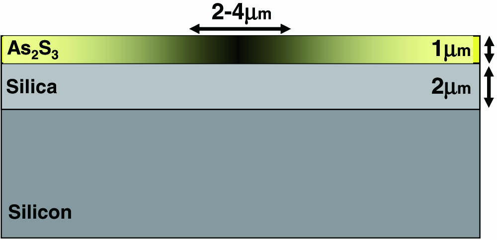
Planar ring resonator waveguides are fabricated in thin films of As2S3 chalcogenide glass, deposited on silica-on-silicon substrates. Waveguide cores are directly written by scanning the focused illumination of a femtosecond Ti:sapphire laser at a central wavelength of 810 nm, through a two-photon photo-darkening process. A large photo-induced index change of 0.3–0.4 refractive index units is obtained. The radius of the ring resonator is 1.9 mm, corresponding to a transmission free spectral range of 9.1 GHz. A high loaded (intrinsic) Q value of 110,000 (180,000) is achieved. The thermal dependence of the resonator transfer function is characterized. The results provide the first report, to the best of our knowledge, of directly written high-Q ring resonators in chalcogenide glass films, and demonstrate the potential of this simple technique towards the fabrication of planar lightguide circuits in these materials.
Glass waveguides Photosensitive materials Resonators Photonics Research
2015, 3(3): 03000063
Author Affiliations
Abstract
1 Department of Information Science and Electronics Engineering, Zhejiang University, Hangzhou 310027, China
2 Cyrus Tang Center for Sensor Materials and Applications, Zhejiang University, Hangzhou 310027, China
In this Letter, we study the characteristics of a selectively buried glass waveguide that is fabricated by the backside masking method. The results show that the surface region appears when the width of the backside mask is larger than 7 mm. Here, the glass substrate is 1.5 mm thick. It is also found that the buried depth evolution of the transition region remains almost unchanged and is independent of the width of the backside mask. The loss of the transition region is only 0.28 dB at the wavelength of 1.55 μm if the surface condition is good enough.
130.0130 Integrated optics 130.2755 Glass waveguides Chinese Optics Letters
2015, 13(2): 021301
集成光电子学国家重点联合实验室(吉林大学实验区),吉林大学电子科学与工程学院,长春 130012
通过K-Na离子交换技术制备了多模玻璃平面波导.采用棱镜耦合技术测量了波导的有效折射率,用IWKB方法拟合得到K-Na离子交换波导的折射率分布符合高斯分布,由色散曲线得到单模波导的制备条件(即扩散深度范围),从而得出单模波导的离子交换时间范围,制备出单模波导,并通过求解WKB色散方程得出单模波导的表面折射率.用普通数码相机,通过对离子交换平面玻璃光波导传输线进行数字成像,根据传输线上的光强分布拟合出光强传输衰减曲线,计算出单模波导的传输损耗大约为0.4 dB/cm.
离子交换 单模玻璃光波导 IWKB法 折射率分布 传输损耗 Ion exchange Single mode glass waveguides Inverse WKB method Refractive index profiles Propagation loss


