

2019, 7(7) Column
Photonics Research 第7卷 第7期

Microscopic pump-probe optical technique to characterize the defect of monolayer transition metal dichalcogenides Download:690次
Download:690次Monolayer transition metal dichalcogenides (TMDs) are ideal materials for atomically thin, flexible optoelectronic and catalytic devices. However, their optoelectrical performance such as quantum yield and carrier mobility often shows below theoretical expectations due to the existence of defects. For monolayer TMD-based devices, finding a low-cost, time-efficient, and nondestructive technique to visualize the change of defect distribution in the space domain and the defect-induced change of the carrier’s lifetime is vital for optimizing their optoelectronic properties. Here, we propose a microscopic pump-probe technique to map the defect distribution of monolayer TMDs. It is found that there is a linear relationship between transient differential reflection intensity and defect density, suggesting that this technique not only realizes the visualization of the defect distribution but also achieves the quantitative estimation of defect density. Moreover, the carrier lifetime at each point can also be obtained by the technique. The technique used here provides a new route to characterize the defect of monolayer TMDs on the micro-zone, which will hopefully guide the fabrication of high-quality two-dimensional (2D) materials and the promotion of optoelectrical performance.


Low-cost hybrid integrated 4 × 25 GBaud PAM-4 CWDM ROSA with a PLC-based arrayed waveguide grating de-multiplexerDownload:781次
Download:781次We demonstrate a low-cost hybrid integrated and compact 100 GBaud four-lane coarse wavelength division multiplexing (CWDM) receiver optical sub-assembly (ROSA) based on an arrayed waveguide grating de-multiplexer in the O band. To achieve the horizontal light coupling between the planar light-wave circuit (PLC) based arrayed waveguide grating de-multiplexer and photodetector array, a 42° polished facet is applied for total reflection. A flexible printed circuit with high-frequency coplanar waveguides is used for a power supply of trans-impedance amplifier and signal transmission. The fabricated CWDM ROSA module, whose size is

In this study, a point-scattering approach to the plane-wave optical transmission of subwavelength metal nanoslit arrays with varying angles of rotation and that of subwavelength metal supercell arrays consisting of nanoslits capable of various angles of rotation is developed. It is demonstrated that the suggested theories show good agreement with the simulations and experiments. The results show that constructive and destructive interference at each nanoslit can respectively enhance and suppress the surface plasmon polariton (SPP) far-field radiation of a metasurface. The proposed theory can predict the quantity and resonant wavelength of SPPs and provide a design scheme for an SPP device.

Tunable and scalable broadband metamaterial absorber involving VO2-based phase transitionDownload:902次
Download:902次Optical absorbers with dynamic tuning features are able to flexibly control the absorption performance, which offers a good platform for realizing optical switching, filtering, modulating, etc. Here, we propose a thermally tunable broadband absorber applying a patterned plasmonic metasurface with thermo-chromic vanadium dioxide (VO 2 VO 2
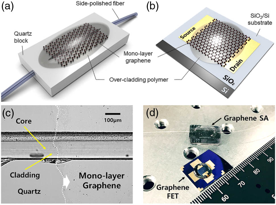
Graphene-based saturable absorber and mode-locked laser behaviors under gamma-ray radiationDownload:582次
Download:582次We investigate optical and electrical behaviors of a graphene saturable absorber (SA) and mode-locking performance of a graphene-SA-based mode-locked Er fiber laser in gamma-ray radiation. When irradiated up to 4.8 kGy at ~ 100 Gy / hr > 10 % > 40
Controlled obtaining of orbital angular momentum (OAM) modes of light at high power over arbitrary orders has important implications for future classical and quantum systems. Appreciable optical amplification has recently been observed for low-order or specific-order OAM modes. However, large amplification of high-order OAM modes still remains challenging. Here we report on flat-gain amplification of arbitrary OAM modes via Brillouin interactions and demonstrate that the OAM modes with various orders can be efficiently and relatively uniformly amplified by imaging the wave source of OAM mode propagation in a nonlinear medium. Meanwhile, the propagation properties of beams carrying OAM with arbitrary modes are high-fidelity maintained. This work provides a practicable way to flatten the mode gain and represents a crucial necessity to realize OAM mode filters with controllable mode gain bandwidth.
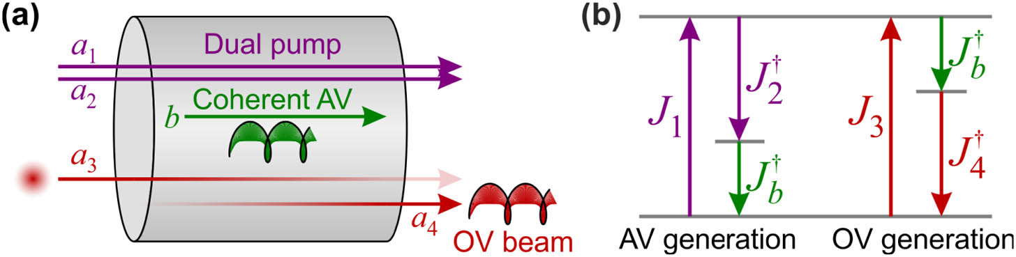
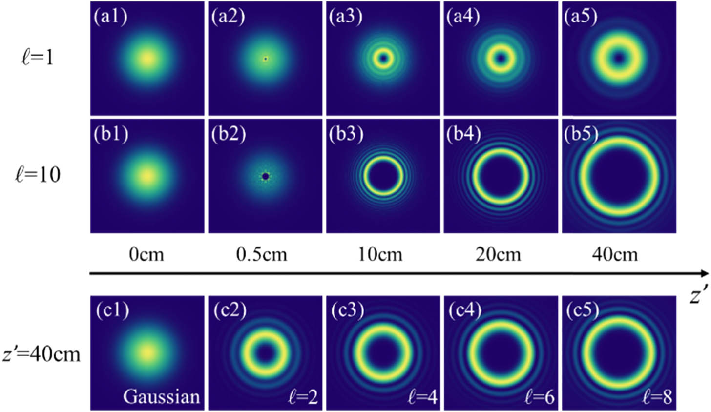
An all-optically reconfigurable generation of optical vortices would be highly beneficial to the implementation of next-generation optical communication and advanced information processing. The previously demonstrated approaches based on the parametric nonlinear optical processes, however, have exhibited limited conversion efficiency due to the group velocity mismatch and nonlinear phase shifts, and require the cumbersome preparation of either the optical element or initial seed beam having a non-zero topological charge. Here, we propose and analyze a novel scheme for highly efficient all-optical generation and control of optical vortices based on the dynamic acoustic vortex grating created by forward stimulated intermodal Brillouin scattering in a subwavelength-hole photonic waveguide. The dual-frequency pump beams in two different hybrid optical modes drive an acoustic vortex mode, which transforms a signal in the fundamental optical mode into an optical vortex mode. This scheme not only eliminates the need for the initial preparation of an angular-momentum-carrying medium or an optical vortex seed but also guarantees high modal purity and nearly 100% conversion efficiency assisted by the energy-momentum conservation. We also investigate the feasibility and practicability of the subwavelength-hole waveguides by examining the intermodal conversion efficiency and robustness of guidance of the optical vortices, taking into account the impact of the Kerr-type nonlinear effects on the intermodal Brillouin interactions based on our rigorous full-vectorial analytical theory.

Layer-modulated two-photon absorption in MoS2: probing the shift of the excitonic dark state and band-edgeDownload:790次
Download:790次Questions hovering over the modulation of bandgap size and excitonic effect on nonlinear absorption in two-dimensional transition metal dichalcogenides (TMDCs) have restricted their application in micro/nano optical modulator, optical switching, and beam shaping devices. Here, degenerate two-photon absorption (TPA) in the near-infrared region was studied experimentally in mechanically exfoliated

Time-domain compact macromodeling of linear photonic circuits via complex vector fittingDownload:528次
Download:528次In this paper, a novel baseband macromodeling framework for linear passive photonic circuits is proposed, which is able to build accurate and compact models while taking into account the nonidealities, such as higher order dispersion and wavelength-dependent losses of the circuits. Compared to a previous modeling method based on the vector fitting algorithm, the proposed modeling approach introduces a novel complex vector fitting technique. It can generate a half-size state-space model for the same applications, thereby achieving a major improvement in efficiency of the time-domain simulations. The proposed modeling framework requires only measured or simulated scattering parameters as input, which are widely used to represent linear and passive systems. Three photonic circuits are studied to demonstrate the accuracy and efficiency of the proposed technique.

Mid-infrared (mid-IR) imaging and spectroscopic techniques have been rapidly evolving in recent years, primarily due to a multitude of applications within diverse fields such as biomedical imaging, chemical sensing, and food quality inspection. Mid-IR upconversion detection is a promising tool for exploiting some of these applications. In this paper, various characteristics of mid-IR upconversion imaging in the femtosecond regime are investigated using a 4 f LiNbO 3

A unique all-fiber interferometric sensor was proposed and successfully demonstrated efficient low-refractive-index liquid sensing in the range from 1.33 to 1.37, which is compatible with those of bio-liquids. A special silica coreless optical fiber with an open V-groove was used as an optical sensing medium, which provided a high sensitivity for a minute liquid volume in the nanoliter scale. The V-groove fiber (VGF) was serially concatenated between two single-mode fibers (SMFs). The LP01 mode guided along the input SMF excited the higher-order modes in the VGF to generate multimode interference, whose spectrum was transmitted through the output SMF. A single liquid droplet with volume of ~ 80

Acousto-optic tunable ultrafast laser with vector-mode-coupling-induced polarization conversionDownload:826次
Download:826次Acousto-optic interactions, employed in the ultrafast laser regulation, possess remarkable advantages for fast tuning performance in a wide spectral range. Here, we propose an ultrafast fiber laser whose wideband tunability is provided by an acousto-optic structure fabricated with an etched single-mode fiber. Because of the laser polarization conversion induced by the coupling between the core and cladding vector modes in the etched fiber, a band-pass characteristic of the acousto-optic interaction is achieved to effectively regulate the inner-cavity gain range. Cooperating with a saturable absorber based on single-wall carbon nanotubes (SWCNTs) with polarization robustness, a soliton operating state is achieved in the tunable erbium-doped fiber laser. By controlling the acoustical wave frequency from 1.039 to 1.069 MHz, this soliton laser can be conveniently tuned in a wide spectral range from 1571.52 to 1539.26 nm. Meanwhile, the laser pulses have near-transform-limited durations stably maintaining less than 2 ps at different wavelength channels, owing to the broadband nonlinear absorption of SWCNTs.

Ultrashort Bessel beam photoinscription of Bragg grating waveguides and their application as temperature sensorsDownload:635次
Download:635次Ultrashort pulsed Bessel beams with intrinsic nondiffractive character and potential strong excitation confinement down to 100 nm can show a series of advantages over Gaussian beams in fabricating efficient Bragg grating waveguides (BGWs). In this work, we focus on parameter management for the inscription of efficient BGWs using the point-by-point method employing Bessel beams. Due to their high aspect ratio, the resulting one-dimensional void-like structures can section the waveguides and interact efficiently with the optical modes. Effective first-order BGWs with low birefringence can then be fabricated in bulk fused silica. By controlling the size and the relative location of grating voids via the Bessel pulse energy and scan velocities, the resonant behaviors of BGWs can be well regulated. A high value of 34 dB for 8 mm length is achieved. A simple predictive model for BGWs is proposed for analyzing the influences of processing parameters on the performance of BGWs. The technique permits multiplexing several gratings in the same waveguide. Up to eight grating traces were straightforwardly inscribed into the waveguide in a parallel-serial combined mode, forming the multiplex BGWs. As an application, the multiplex BGW sensor with two resonant peaks is proposed and fabricated for improving the reliability of temperature detection.

Enhancing sensitivity to ambient refractive index with tunable few-layer graphene/hBN nanoribbonsDownload:649次
Download:649次Refractive index (RI) sensing helps to identify biomolecules and chemicals in the mid-infrared range for drug discovery, bioengineering, and environmental monitoring. In this paper, we numerically demonstrate an electrically tunable RI sensor with ultrahigh sensitivity using a three-layer graphene nanoribbon array separated by hexagonal boron nitride (hBN). Unlike the weak resonance in single-layer graphene nanoribbons, a much stronger plasmon resonance featuring a higher-quality factor can be excited in the graphene/hBN few-layer ribbon array. Simultaneously, the high purity of graphene on hBN results in an outstanding charge mobility above 4 × 10 4 cm 2 · V 1 · s 1

Quantum information protocols often rely on tomographic techniques to determine the state of the system. A popular method of encoding information is on the different paths a photon may take, e.g., parallel waveguides in integrated optics. However, reconstruction of states encoded onto a large number of paths is often prohibitively resource intensive and requires complicated experimental setups. Addressing this, we present a simple method for determining the state of a photon in a superposition of d 0.9852 ± 0.0008
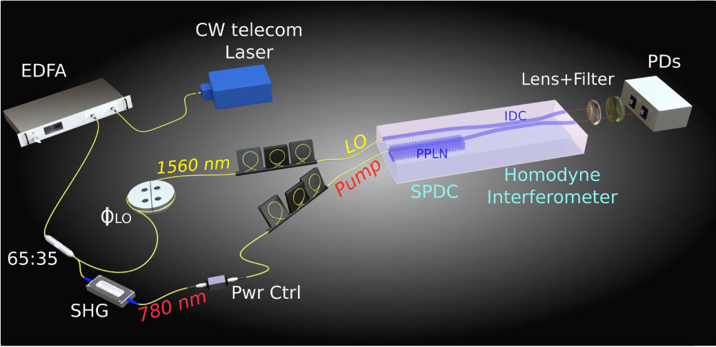
We demonstrate a squeezing experiment exploiting the association of integrated optics and telecom technology as key features for compact, stable, and practical continuous variable quantum optics. In our setup, squeezed light is generated by single-pass spontaneous parametric down conversion on a lithium niobate photonic circuit and detected by a homodyne detector whose interferometric part is directly integrated on the same platform. The remaining parts of the experiment are implemented using commercial plug-and-play devices based on guided-wave technologies. We measure, for a CW pump power of 40 mW, a squeezing level of 2.00 ± 0.05 dB 2.80 ± 0.05 dB

The impact of operation current on the degradation behavior of 310 nm UV LEDs is investigated over 1000 h of stress. It ranges from 50 to 300 mA and corresponds to current densities from 34 to 201 A / cm 2

1 Gbps free-space deep-ultraviolet communications based on III-nitride micro-LEDs emitting at 262 nmDownload:787次
Download:787次The low modulation bandwidth of deep-ultraviolet (UV) light sources is considered as the main reason limiting the data transmission rate of deep-UV communications. Here, we present high-bandwidth III-nitride micro-light-emitting diodes (μLEDs) emitting in the UV-C region and their applications in deep-UV communication systems. The fabricated UV-C μLEDs with

影响因子:7.6
CN:31-2126/O4
ISSN:2327-9125


公告
动态信息
动态信息 丨 2024-04-25
PR Highlight (Vol. 12, Iss. 2): 封面|超紧凑片上偏振控制器动态信息 丨 2024-04-11
PR Highlight (Vol. 11, Iss. 12): 亮点 | 十亿像素级、高通量的无透镜偏振编码叠层成像技术动态信息 丨 2024-03-29
PR 封面故事 (Vol. 12, Iss. 3): 封面 | 基于时空编码神经网络的像差感知超分辨成像动态信息 丨 2024-03-25
PR 封面故事 (Vol. 12, Iss. 1) 光涡旋与手性器件微纳3D打印动态信息 丨 2024-03-14
PR Highlight (Vol. 12, Iss. 1): 同步双脉冲激光烧蚀中的气泡相互作用效应激光评论微信公众号

点击菜单“联系编辑”即可添加期刊编辑为好友啦