Photonics Research, 2019, 7 (3): 03000294, Published Online: Feb. 20, 2019  

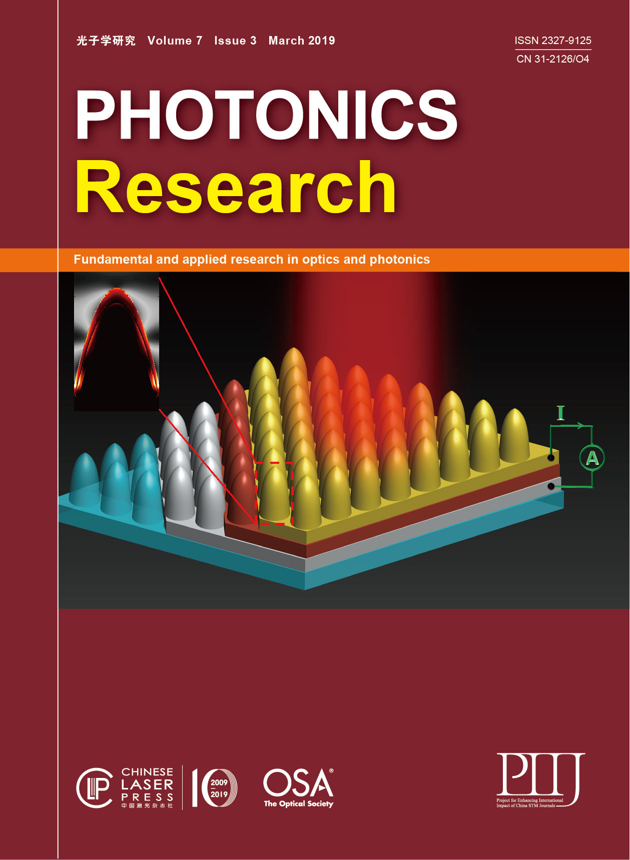
Silica nanocone array as a template for fabricating a plasmon induced hot electron photodetector Download: 578次

Author Affiliations
1 Key Laboratory of Space Applied Physics and Chemistry, Ministry of Education, and Shaanxi Key Laboratory of Optical Information Technology, School of Science, Northwestern Polytechnical University, Xi’an 710072, China
2 Department of Electrical and Computer Engineering, National University of Singapore, Singapore 117583, Singapore
3 LEES Program, Singapore-MIT Alliance for Research & Technology (SMART), Singapore 138602, Singapore
Copy Citation Text

Zhiqiang Yang, Kang Du, Fanfan Lu, Yang Pang, Shijia Hua, Xuetao Gan, Wending Zhang, Soo Jin Chua, Ting Mei. Silica nanocone array as a template for fabricating a plasmon induced hot electron photodetector[J]. Photonics Research, 2019, 7(3): 03000294.

References

[1] Y. Takahashi, T. Tatsuma. Solid state photovoltaic cells based on localized surface plasmon-induced charge separation. Appl. Phys. Lett., 2011, 99: 182110.

[2] Y. K. Lee, H. Lee, C. Lee, E. Hwang, J. Y. Park. Hot-electron-based solar energy conversion with metal–semiconductor nanodiodes. J. Phys. Condens. Matter, 2016, 28: 254006.

[3] J. M. Stern, J. Stanfeld, W. Kabbani, J.-T. Hsieh, J. A. Cadeddu. Selective prostate cancer thermal ablation with laser activated gold nanoshells. J. Urol., 2008, 179: 748-753.

[4] S. Mubeen, J. Lee, N. Singh, S. Kramer, G. D. Stucky, M. Moskovits. An autonomous photosynthetic device in which all charge carriers derive from surface plasmons. Nat. Nanotechnol., 2013, 8: 247-251.

[5] S. Mukherjee, F. Libisch, N. Large, O. Neumann, L. V. Brown, J. Cheng, J. B. Lassiter, E. A. Carter, P. Nordlander, N. J. Halas. Hot electrons do the impossible: plasmon-induced dissociation of H2 on Au. Nano Lett., 2013, 13: 240-247.

[6] W. Li, J. G. Valentine. Harvesting the loss: surface plasmon-based hot electron photodetection. Nanophotonics, 2017, 6: 177-191.

[7] Y. P. Huang, L. A. Wang. In-line silicon Schottky photodetectors on silicon cored fibers working in 1550 nm wavelength regimes. Appl. Phys. Lett., 2015, 106: 191106.

[8] S. Muehlbrandt, A. Melikyan, T. Harter, K. Köhnle, A. Muslija, P. Vincze, S. Wolf, P. Jakobs, Y. Fedoryshyn, W. Freude, J. Leuthold, C. Koos, M. Kohl. Silicon-plasmonic internal-photoemission detector for 40  Gbit/s data reception. Optica, 2016, 3: 741-747.

[9] Z. Yang, M. Liu, S. Liang, W. Zhang, T. Mei, D. Zhang, S. J. Chua. Hybrid modes in plasmonic cavity array for enhanced hot-electron photodetection. Opt. Express, 2017, 25: 20268-20273.

[10] T. Gong, J. N. Munday. Aluminum-based hot carrier plasmonics. Appl. Phys. Lett., 2017, 110: 021117.

[11] Y. Liu, X. Zhang, J. Su, H. Li, Q. Zhang, Y. Gao. Ag nanoparticles@ZnO nanowire composite arrays: an absorption enhanced UV photodetector. Opt. Express, 2014, 22: 30148-30155.

[12] H. Li, X. Zhang, N. Liu, L. Ding, J. Tao, S. Wang, J. Su, L. Li, Y. Gao. Enhanced photo-response properties of a single ZnO microwire photodetector by coupling effect between localized Schottky barriers and piezoelectric potential. Opt. Express, 2015, 23: 21204-21212.

[13] M. L. Brongersma, N. J. Halas, P. Nordlander. Plasmon-induced hot carrier science and technology. Nat. Nanotechnol., 2015, 10: 25-34.

[14] H. Chalabi, M. L. Brongersma. Plasmonics: harvest season for hot electrons. Nat. Nanotechnol., 2013, 8: 229-230.

[15] I. Goykhman, B. Desiatov, J. Khurgin, J. Shappir, U. Levy. Locally oxidized silicon surface-plasmon Schottky detector for telecom regime. Nano Lett., 2011, 11: 2219-2224.

[16] Y. K. Lee, C. H. Jung, J. Park, H. Seo, G. A. Somorjai, J. Y. Park. Surface plasmon-driven hot electron flow probed with metal-semiconductor nanodiodes. Nano Lett., 2011, 11: 4251-4255.

[17] B. Desiatov, I. Goykhman, N. Mazurski, J. Shappir, J. B. Khurgin, U. Levy. Plasmonic enhanced silicon pyramids for internal photoemission Schottky detectors in the near-infrared regime. Optica, 2015, 2: 335-338.

[18] M. W. Knight, Y. Wang, A. S. Urban, A. Sobhani, B. Y. Zheng, P. Nordlander, N. J. Halas. Embedding plasmonic nanostructure diodes enhances hot electron emission. Nano Lett., 2013, 13: 1687-1692.

[19] W. Li, Z. J. Coppens, L. V. Besteiro, W. Wang, A. O. Govorov, J. Valentine. Circularly polarized light detection with hot electrons in chiral plasmonic metamaterials. Nat. Commun., 2015, 6: 8379.

[20] M. W. Knight, H. Sobhani, P. Nordlander, N. J. Halas. Photodetection with active optical antennas. Science, 2011, 332: 702-704.

[21] A. Sobhani, M. W. Knight, Y. Wang, B. Zheng, N. S. King, L. V. Brown, Z. Fang, P. Nordlander, N. J. Halas. Narrowband photodetection in the near-infrared with a plasmon-induced hot electron device. Nat. Commun., 2013, 4: 1643.

[22] K. T. Lin, H. L. Chen, Y. S. Lai, C. C. Yu. Silicon-based broadband antenna for high responsivity and polarization-insensitive photodetection at telecommunication wavelengths. Nat. Commun., 2014, 5: 3288.

[23] W. Li, J. Valentine. Metamaterial perfect absorber based hot electron photodetection. Nano Lett., 2014, 14: 3510-3514.

[24] F. Pelayo García de Arquer, A. Mih, G. Konstantatos. Large-area plasmonic-crystal-hot-electron-based photodetectors. ACS Photon., 2015, 2: 950-957.

[25] H. Lee, Y. K. Lee, E. Hwang, J. Y. Park. Enhanced surface plasmon effect of Ag/TiO2 nanodiodes on internal photoemission. J. Phys. Chem. C, 2014, 118: 5650-5656.

[26] M. G. Ramchandani. Energy band structure of gold. J. Phys. C, 1970, 3: 1S.

[27] P. Moitra, B. A. Slovick, W. Li, I. I. Kravchencko, D. P. Briggs, S. Krishnamurthy, J. Valentine. Large-scale all-dielectric metamaterial perfect reflectors. ACS Photon., 2015, 2: 692-698.

[28] P. Gao, J. He, S. Zhou, X. Yang, S. Li, J. Sheng, D. Wang, T. Yu, J. Ye, Y. Cui. Large-area nanosphere self-assembly by a micro-propulsive injection method for high throughput periodic surface nanotexturing. Nano Lett., 2015, 15: 4591-4598.

[29] C.-M. Hsu, S. T. Connor, M. X. Tang, Y. Cui. Wafer-scale silicon nanopillars and nanocones by Langmuir–Blodgett assembly and etching. Appl. Phys. Lett., 2008, 93: 133109.

[30] J. Hao, L. Zhou, M. Qiu. Nearly total absorption of light and heat generation by plasmonic metamaterials. Phys. Rev. B, 2011, 83: 165107.

[31] R. H. Fowler. The analysis of photoelectric sensitivity curves for clean metals at various temperatures. Phys. Rev., 1931, 38: 45-56.

[32] C. Scales, P. Berini. Thin-film Schottky barrier photodetector models. IEEE J. Quantum Electron., 2010, 46: 633-643.

[33] C. Clavero. Plasmon-induced hot-electron generation at nanoparticle/metal-oxide interfaces for photovoltaic and photocatalytic devices. Nat. Photonics, 2014, 8: 95-103.

[34] H. Chalabi, D. Schoen, M. L. Brongersma. Hot-electron photodetection with a plasmonic nanostripe antenna. Nano Lett., 2014, 14: 1374-1380.

[35] T. Gong, J. N. Munday. Angle-independent hot carrier generation and collection using transparent conducting oxides. Nano Lett., 2015, 15: 147-152.

[36] J. G. Simmons. Generalized formula for the electric tunnel effect between similar electrodes separated by a thin insulating film. J. Appl. Phys., 1963, 34: 1793-1803.

[37] J. C. Fisher, I. Giaever. Tunneling through thin insulating layers. J. Appl. Phys., 1961, 32: 172-177.

Zhiqiang Yang, Kang Du, Fanfan Lu, Yang Pang, Shijia Hua, Xuetao Gan, Wending Zhang, Soo Jin Chua, Ting Mei. Silica nanocone array as a template for fabricating a plasmon induced hot electron photodetector[J]. Photonics Research, 2019, 7(3): 03000294.

引用该论文: TXT   |   EndNote

相关论文

加载中...

关于本站 Cookie 的使用提示

中国光学期刊网使用基于 cookie 的技术来更好地为您提供各项服务,点击此处了解我们的隐私策略。 如您需继续使用本网站,请您授权我们使用本地 cookie 来保存部分信息。
全站搜索
您最值得信赖的光电行业旗舰网络服务平台!