1. INTRODUCTION
In recent years, hot electrons have attracted enthusiastic attention due to their excellent potential applications in solar cells [1,2], bio-optics [3,4], chemical catalysis [5], and photoelectric detection [6–12" target="_self" style="display: inline;">–12]. In general, the efficiency of exciting hot electrons by photons directly incident on a planar metal is too low. However, when light is incident on a metal with a nanostructure to generate surface plasmons (SPs), the SPs will significantly enhance the light absorption by the metal, and a large number of hot electrons are generated during the nonradiative decay process of the plasmons [13]. If the plasmonic metal is applied on a semiconductor (or a thin layer of insulator deposited on another metal), a portion of the hot electrons can be emitted over the Schottky barrier into the conduction band of the semiconductor (metal–semiconductor, MS) or over the thin-layer insulator (metal–insulator–metal, MIM) in contact with the metal [6,14]. The main advantage of hot electron optoelectronic devices is that they are capable of detecting light well below the bandgap of the semiconductor [1517" target="_self" style="display: inline;">–17], and the response spectrum is tunable based on the configuration of the plasmonic metal nanostructure [18,19].
So far there are three ways to fabricate plasmonic metal nanostructures using MS or MIM structures for use in hot electron photodetectors. The first method is to use electron beam lithography (EBL) to prepare the nanostructures. This method has created metal plasmonic nanostructures to excite SP polaritons (SPPs) or local SP resonance (LSPR), such as a nanoantenna [20], grating [21], deep trench [22], and metasurface [23]. The disadvantage of this method is that the fabrication process cost is high. The second method is to use soft nanoimprinting lithography. Gerasimos achieved controllable plasmonic crystals with a tunable response across the visible and near-infrared wavelengths [24]. The third method is the self-assembly of random nanostructures, such as the annealing of thin metal films [25] to form nanoislands. However, the plasmonic response obtained with random structures is not as high as the other two methods.
Here, we present the first implementation, to the best of our knowledge, of a hot electron photodetector made with polystyrene (PS) nanosphere lithography and compatible for fabricating large devices. It is a low cost alternative to nanoimprinting, giving equally good results. A nanocone array (NCA) is formed on a silica substrate. Based on this template, a MS–metal (MSM) structure was fabricated. Inductively coupled plasma (ICP) was used to etch the PS masked silica to form an NCA, which was then plated with aluminum (Al), titanium dioxide () (semiconductor), and gold (Au) films sequentially, to fabricate an MSM structure. Al and Au counter-electrodes are separated by a thin layer of formed by atomic layer deposition (ALD). The plasmon excited hot electrons in Au can tunnel through the layer and eventually reach the Al electrode to form a circuit. This device exhibits a strong photoelectric response at around 620 nm. In the short-wavelength region (400–620 nm), the calculated and experimental responsivities diverge as a consequence of the absorption of electrons in the Au band [26]. In contrast, they are in good agreement in the long-wavelength region (620–1000 nm). In addition to these experimental results at zero bias, the response can be significantly enhanced under reverse bias. The red shifts in the response peak with an increase in bias indicate that the bias causes an increase in the hot electron tunneling effect. The change in response with bias voltage is in good agreement with theory. The implementation of PS nanosphere lithography to fabricate an array of nanocones for use in photodetection will be advantageous for integration on a vast variety of optoelectronic and microelectronic devices.
2. EXPERIMENTAL SETUP AND METHODS
PS nanospheres that are 400 nm in diameter were self-assembled into a monolayer hexagonal close-packed lattice on silica wafers by the Langmuir–Blodgett (LB) assembly method [2729" target="_self" style="display: inline;">–29]. Then, the wafers with the PS nanosphere mask layer were etched with ICP for 9 min durations at 0.5 mTorr (1 Torr = 133.322 Pa) pressure, 30 W RF power, 1500 W ICP power, and 4 standard cubic centimeters per minute (SCCM) flow rate. At this step, NCA was formed on the silica surface. After that, the residual PS nanospheres on the silica surface were removed by annealing at 450°C for 5 min. On the NCA, 80 nm thick Al, 8 nm , and 60 nm Au were sequentially deposited. was deposited by ALD with water and titanium isopropoxide used as the precursors and open valve durations of 0.2 and 0.02 s, respectively, followed by a 30 s pump down. The chamber was kept at 250°C during the deposition process. This gives a thickness of 0.02 nm per cycle. Au and Al were deposited by double target and double angle thermal evaporation to ensure that the metal films are conformal. The evaporation rate is at a base pressure lower than .
The device was characterized under ambient conditions. Current–voltage characteristics were recorded with a Keithley 2400 source meter. The spectral characterization was carried out by illuminating the devices with a HORIBA iHR 320 monochromator, modulated by a 200 Hz chopper, and monitoring the current with a Stanford research system SR830 apparatus. The light source was a 100 W quartz tungsten halogen lamp (Newport 66877-100Q-H). Long-pass filters (400 nm cutoff, Thorlabs) were used in the measurement of the spectral photoresponse.
3. RESULTS AND DISCUSSION
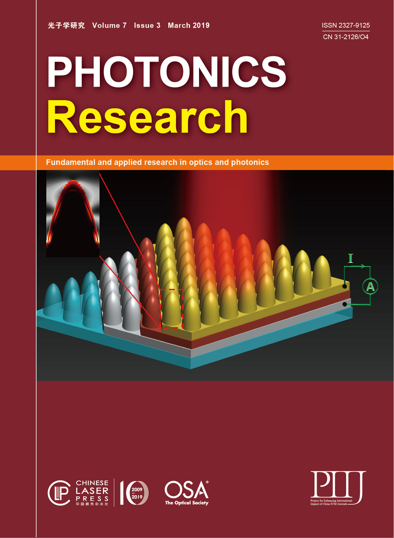
The final architecture of the NCA-based photodetector is represented in Fig. 1(a). When illuminated from the top of the sample, the Au layer due to the presence of NCA SPs will be excited on the Au layer. Then, the hot electrons excited by SPs pass through the Schottky barrier formed at the Au and interface. They enter the conduction band of and are eventually collected by the other side of the Al electrode [Fig. 1(b)]. Figure 1(c) shows the photograph of large-scale etched silica NCA. The green color observable with the naked eye results from diffraction associated with the periodicity of NCA. The top view and cross-sectional scanning electron microscope (SEM) images of the device are shown in Figs. 1(d) and 1(e), respectively. The large-area hexagonal NCA has a period slightly larger than the diameter of the PS nanospheres (about 430 nm), and the height of the nanocone is about 460 nm.
Fig. 1. Device architecture and principle of operation. (a) Representation of the NCA photodetector. Light impinges on the top Au film, exciting hot electrons through SP generation. The color of the cones corresponds to the layer with the same color shown in (b). (b) Transport process of hot electrons. (c) Etched silicon dioxide with a 400 nm PS nanosphere mask on a sample. The green color is due to the reflected light from the nanostructured surface, whereas the dark area is the unetched silicon oxide. (d) Top view and (e) cross-sectional SEM image of the final device.
下载图片 查看所有图片
To understand the optical properties of the NCA device, a finite-difference-time-domain (FDTD) simulation was performed to calculate the light absorption as well as electric field distribution. Figure 2(a) shows the simulated absorption spectrum of the device. In the region of 400–500 nm, the absorption rate of the device reaches 0.9 or more, which is mainly due to the interband absorption of Au -band electrons. As the wavelength exceeds 600 nm, the interband absorption is no longer important, and the main mechanism is entirely due to the free electron absorption; hence, the absorption is significantly reduced. The electric field diagram of the NCA device at 620 nm is shown in Fig. 2(b). Owing to the presence of the nanostructures, SPs can be excited by the incident electromagnetic waves and propagate along the Au surface, resulting in enhanced absorption by the Au films. Although the electric field is slightly enhanced at the base of the nanocone, the propagating SP mode is the main absorbing mechanism leading to the loss of -band absorption, thus resulting in a significant decline in the overall absorption rate. To gain insight into the nature of absorption distribution, we calculated the time-averaged dissipative energy density numerically at the nanocone using [30] where ) is the local electric field, and is the imaginary part of the metal permittivity. As shown in Fig. 2(c), the absorption is mainly concentrated in the Au layer due to the SPP excitation at the Au–air interface. The intermediate layer of acts as a dielectric layer and does not absorb any energy. The lower electrode, i.e., the Al layer, also absorbs a small portion of the energy, but the number of hot electrons generated in the Au layer will be much larger than that in the Al layer, allowing this structure to generate a net current from Au to Al.
Fig. 2. (a) Calculated absorbance spectrum in the 400–1000 nm range. (b) Simulated electric-field intensity distribution at the cross-section at the wavelength of 620 nm. (c) Distribution of dissipative energy density at the wavelength of 620 nm, showing strong absorption along the sidewall.
下载图片 查看所有图片
The Au layer thickness is an important parameter of the hot electron device. In order to obtain the optimized thickness of the Au layer and the thickness of , we prepare several NCA devices with 30, 40, 50, 60, 70, and 80 nm Au layers, a 4 nm layer, and a 80 nm Al layer for the experiments. Figure 3 shows that the photocurrent is generated when exposed to a wide-spectrum source. Keeping all other measurement parameters constant, it can be seen that the thickness with 60 nm gives the largest photocurrent. Furthermore, we measure the photocurrent spectral response of these samples. The results show that the photocurrent spectral response shows similar features, except for their intensities. In another experiment, we made layers with thicknesses of 2, 4, 6, 8, and 10 nm and finally selected 8 nm as the thickness of in the experiment.
Fig. 3. Photocurrent varies with the thickness of the Au layer.
下载图片 查看所有图片
We then sought to experimentally assess the optoelectronic spectral response of the NCA device (Au 60 nm, 8 nm, Al 80 nm). The responsivity measured under short-circuit conditions is shown in Fig. 4(a), where a broad band response is obtained between 500 and 900 nm wavelengths and exhibits a strong photoelectric response of 180 μA/W around 620 nm. The energy gap of is 3.2 eV, and the thickness is only 8 nm; we can thus believe that the current must be from the SP excited hot electrons. Assuming that the reverse current provided by the hot electrons in the Al electrode is ignored, there are two reasons for this: one is that the Al electrode absorbance is quite small, and another is that the contact is close to the ohmic contact. The relationship between the responsivity and the absorption is given by the Fowler formula [31,32]: where is the Fowler coefficient, is the photon energy, q is the elemental charge, and is the effective Schottky barrier height, which we estimated to be 0.81 eV from current–voltage measurements. The calculated responsivity is shown in Fig. 4(a). In the wavelength region larger than 600 nm, the calculated and experimental responsivities are in good agreement, but, at wavelengths below , the calculated and experimental responsivities diverge as a consequence of the increasing contribution of the interband transitions. To analyze its internal mechanism, we provide a theoretical energy band diagram [Fig. 4(b)]. The band of Au is 2.4 eV below the Fermi level [33], even at the highest photon energy of 400 nm (3.1 eV). The energy of hot electrons can only reach 0.7 eV at most, where they are still not able to cross the Schottky barrier. When is larger than 600 nm, the hot electrons are excited by free electrons near the Fermi level, and the hot electrons passing through the barrier can still be excited at (1.24 eV).
Fig. 4. (a) Responsivity under short-circuit conditions. (b) Band diagram of Au showing excitation from different bands. Hot electrons with energy larger than the Schottky barrier can be emitted over the barrier into the semiconductor.
下载图片 查看所有图片
We next characterize the performance of the NCA device under bias. Responsivity under short-circuit conditions is low for practical application, which is a common drawback for hot electron devices. The application of a reverse bias to the junction could in principle overcome the low injection yield because the associated decrease in the barrier height favors efficient hot electron injection. Figure 5(a) is an equivalent circuit diagram of the device under bias. As shown on the energy band diagram [Figs. 5(b) and 5(c)], under short-circuit conditions, only the fraction of those hot electrons that can reach the interface with enough momentum are tunneling candidates. Under reverse bias, that is, with the Au electrode biased at a negative voltage, the main voltage drop falls in the layer. The barrier profile is modulated, resulting in an increase in the bending of the conduction band and, thus, the lowering of the barrier of the triangular region, allowing more hot electrons to cross the Schottky barrier.
Fig. 5. (a) Equivalent circuit diagram of the device under bias. (b) Schematic of hot electrons transported across the Schottky barrier under short-circuit conditions. (c) Schematic of hot electrons tunneling under reverse bias. As the reverse bias increases, the barrier profile is modulated as their alternating bands are pushed downward. (d) Responsivity under different reverse biases. (e) Relationship between the photocurrent and the bias voltage under 620 nm illumination.
下载图片 查看所有图片
To experimentally assess this improvement, the device responsivity as a function of illumination wavelengths is shown in Fig. 5(d) for different reverse biases. It can be seen that as the bias voltage increases, a higher fraction of the excited electrons can overcome the barrier, increasing the responsivity as the reverse bias is increased. A similar behavior was also reported in MIM hot electron devices [34,35]. The increase in responsivity is accompanied by a slight red shift in the response peak, which we speculate is due to the increased current contributed by tunneling of lower-energy electrons under bias [Fig. 5(c)]. Figure 5(e) shows the relationship between the photocurrent and the bias voltage under the 620 nm light source. As the voltage increases, the photocurrent increases exponentially. When the bias voltage reaches 0.8 eV, the photocurrent increases faster. The reason is that as the reverse bias approaches , the injection probability can be substantially improved [36]. The increasing trend is qualitatively confirmed by a theoretical model of tunneling through a bias-dependent barrier [37].
4. CONCLUSIONS
We present a robust and novel architecture for visible-infrared photodetection based on hot electron injection from plasmonic NCAs formed by self-assembled PS nanosphere lithography. The device is based on a silica template that allows fabrication to be compatible with other Si-based devices. The photon absorption is mainly contributed by the Au layer at the sidewalls of the nanocones. This absorption is not due to local SP excitation but due to SPP at the Au–air interface. The responsivity under short-circuit conditions shows a peak of 180 μA/W at about 620 nm, which indicates that a significant fraction of the excited carriers can be collected. Under reverse bias operation, the responsivity shows a tendency to increase with bias and red shift in the peak value due to the tunneling effect. When the reverse bias is equal to 1 V, our devices yield responsivity of up to 360 μA/W.
The response of the device could be further improved by increasing the reverse bias voltage. Also, other semiconductors such as zinc oxide and a metal such as silver may be used on the silica NCA template to adjust the Schottky barrier height. Based on these concepts, our devices have the potential to be used for sub-bandgap photodetection in other wavelength bands. NCAs can be applied in other areas such as photovoltaics or photocatalysis with the advantage of being able to fabricate large-area devices at much lower costs.
5 Acknowledgment
Acknowledgment. We thank the Analytical & Testing Center of Northwestern Polytechnical University for support in device fabrication and characterization.
Zhiqiang Yang, Kang Du, Fanfan Lu, Yang Pang, Shijia Hua, Xuetao Gan, Wending Zhang, Soo Jin Chua, Ting Mei. Silica nanocone array as a template for fabricating a plasmon induced hot electron photodetector[J]. Photonics Research, 2019, 7(3): 03000294.
 Download: 577次
 Representation of the NCA photodetector. Light impinges on the top Au film, exciting hot electrons through SP generation. The color of the cones corresponds to the layer with the same color shown in (b). (b) Transport process of hot electrons. (c) Etched silicon dioxide with a 400 nm PS nanosphere mask on a 1.5 cm×1.5 cm sample. The green color is due to the reflected light from the nanostructured surface, whereas the dark area is the unetched silicon oxide. (d) Top view and (e) cross-sectional SEM image of the final device.")
 Calculated absorbance spectrum in the 400–1000 nm range. (b) Simulated electric-field intensity distribution at the cross-section at the wavelength of 620 nm. (c) Distribution of dissipative energy density at the wavelength of 620 nm, showing strong absorption along the sidewall.")

 Responsivity under short-circuit conditions. (b) Band diagram of Au showing excitation from different bands. Hot electrons with energy larger than the Schottky barrier can be emitted over the barrier into the semiconductor.")
 Equivalent circuit diagram of the device under bias. (b) Schematic of hot electrons transported across the Schottky barrier under short-circuit conditions. (c) Schematic of hot electrons tunneling under reverse bias. As the reverse bias increases, the barrier profile is modulated as their alternating bands are pushed downward. (d) Responsivity under different reverse biases. (e) Relationship between the photocurrent and the bias voltage under 620 nm illumination.")


 PDF全文
PDF全文

