Photonics Research, 2019, 7 (3): 03000294, Published Online: Feb. 20, 2019
Silica nanocone array as a template for fabricating a plasmon induced hot electron photodetector  Download: 578次
Figures & Tables
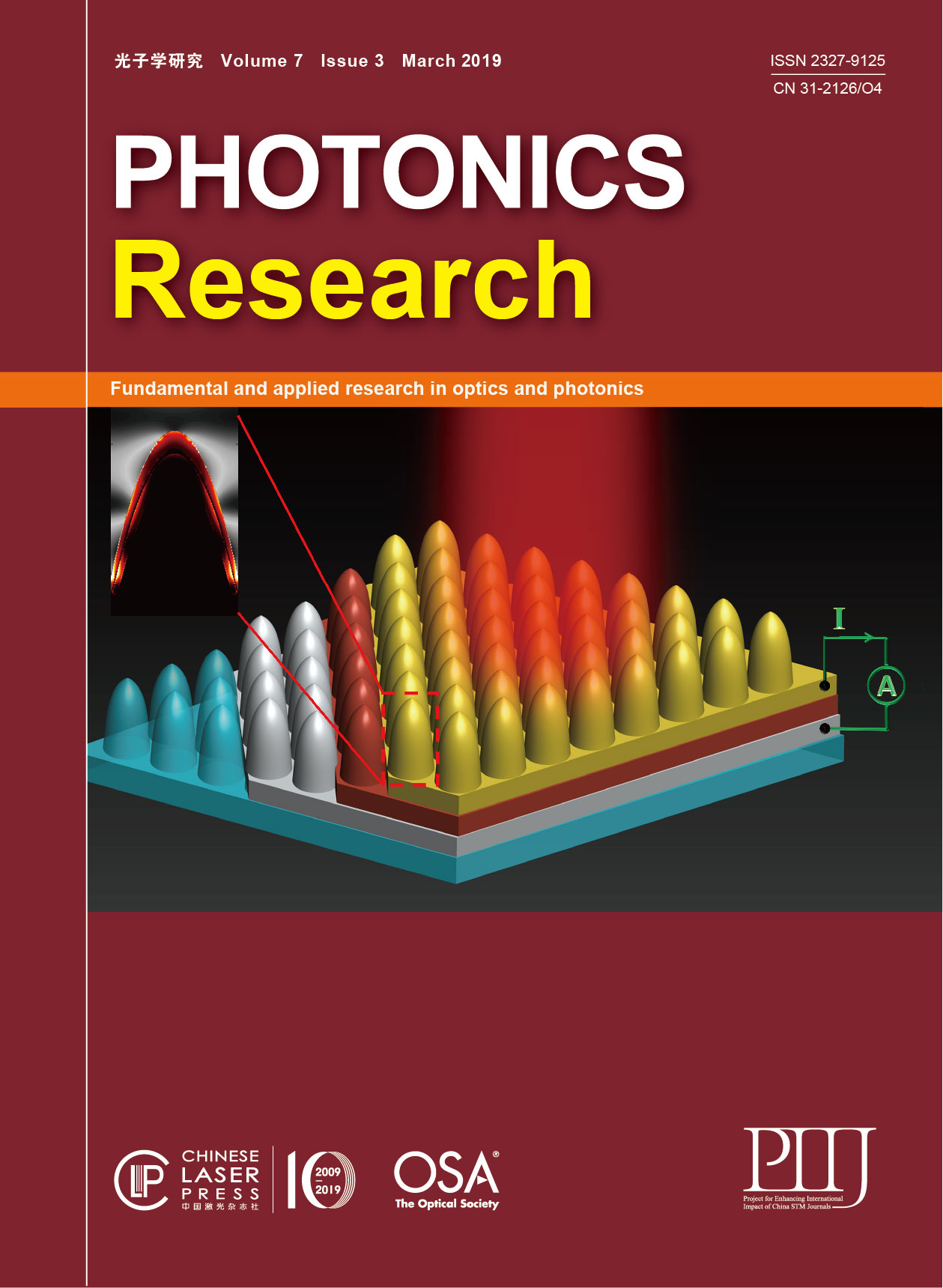
Fig. 1. Device architecture and principle of operation. (a) Representation of the NCA photodetector. Light impinges on the top Au film, exciting hot electrons through SP generation. The color of the cones corresponds to the layer with the same color shown in (b). (b) Transport process of hot electrons. (c) Etched silicon dioxide with a 400 nm PS nanosphere mask on a 1.5 cm × 1.5 cm

Fig. 2. (a) Calculated absorbance spectrum in the 400–1000 nm range. (b) Simulated electric-field intensity distribution at the cross-section at the wavelength of 620 nm. (c) Distribution of dissipative energy density at the wavelength of 620 nm, showing strong absorption along the sidewall.


Fig. 4. (a) Responsivity under short-circuit conditions. (b) Band diagram of Au showing excitation from different bands. Hot electrons with energy larger than the Schottky barrier can be emitted over the barrier into the semiconductor.

Fig. 5. (a) Equivalent circuit diagram of the device under bias. (b) Schematic of hot electrons transported across the Schottky barrier under short-circuit conditions. (c) Schematic of hot electrons tunneling under reverse bias. As the reverse bias increases, the barrier profile is modulated as their alternating bands are pushed downward. (d) Responsivity under different reverse biases. (e) Relationship between the photocurrent and the bias voltage under 620 nm illumination.

Zhiqiang Yang, Kang Du, Fanfan Lu, Yang Pang, Shijia Hua, Xuetao Gan, Wending Zhang, Soo Jin Chua, Ting Mei. Silica nanocone array as a template for fabricating a plasmon induced hot electron photodetector[J]. Photonics Research, 2019, 7(3): 03000294.


 PDF全文
PDF全文

