1 School of Physics and Optoelectronics, South China University of Technology, Guangzhou 510640, China
2 School of Electronic and Information Engineering, South China University of Technology, Guangzhou 510640, China
Abstract
We have studied a switchable hyperbolic metamaterial composed of a graphene–dielectric periodic structure. By tuning the chemical potential of all graphene sheets simultaneously, the isofrequency curve can switch between an ellipse and a hyperbola conveniently. In particular, a special hyperbolic isofrequency curve with its asymptote perpendicular to the interface is obtained and used to realize the zero reflection effect. Furthermore, a zero-reflection-based optical switch working in the terahertz spectrum is demonstrated. Its bandwidth can be efficiently adjusted by geometric parameters such as permittivity and period. Such an optical switch possesses the merits of low loss, high transmittance contrast, high response speed, compact size, high tolerance of chemical potential, and having all incident angles (0°–90°) simultaneously. Such an optical switch holds great potential in many fields, such as data storage, beam steering, and integrated photonic circuits.
1. INTRODUCTION
Metamaterials, which are artificial subwavelength structured materials, have been a hot topic of central importance due to their properties never observed in nature [13" target="_self" style="display: inline;">–3]. Among them, hyperbolic metamaterials are one of the most unusual classes of metamaterials [4,5]. Hyperbolic metamaterials have a diagonal permittivity tensor (or permeability tensor) whose principal components possess opposite signs. This special feature leads to its unusual hyperbolic dispersion and many unique properties. Unlike conventional double-negative metamaterials realized by a resonant-mediated mechanism, hyperbolic metamaterials not only simplify structures, but also make tunability possible. Hyperbolic metamaterials have attracted growing attention recently, whose applications involve negative refraction [68" target="_self" style="display: inline;">–8], nano-scale waveguides [9,10], sub-wavelength imaging [11], and spontaneous emission [12,13].
Metal is the most common material used to fabricate hyperbolic metamaterials, and the most common structures are nanowire-array structures [14] and layered metal–dielectric structures [15]. For example, the zero reflection effect in a metal–dielectric metamaterial was studied [16]. However, an inherent problem of such a metal-structured composite is material loss. Moreover, it is difficult to control the permittivity of metals after fabrication. Overcoming these two drawbacks is highly desired. Magnetic metamaterial based on YIG–dielectric layered structure is another kind of hyperbolic metamaterial, and it is used for optical switch design [17]; however, its modulation speed is low, and it works only in the microwave spectrum, since it does not have a magnetic response in infrared and terahertz spectra. What is more, it requires a bulky magnetic field unit for control, which is not convenient for practical applications and is unfavorable for miniaturization. In contrast to metal, graphene, a one-atom-thick allotrope of carbon first discovered in 2004 [18], is lossless and has excellent electronic and optical properties in infrared and terahertz spectra. Furthermore, its dielectric permittivity can be tuned by chemical potential, Fermi energy, external electrostatic field biasing, gate voltage, magnetic field, chemical doping, or the nonlinear effect [19–24" target="_self" style="display: inline;">–24], so graphene is a good candidate for overcoming the aforementioned drawbacks of metal and can work in infrared and terahertz spectra, which is favorable for on-chip integration. Recently, multilayer structures consisting of graphene and dielectric have been studied as tunable hyperbolic metamaterials [25–29" target="_self" style="display: inline;">–29]. The topological transitions and associated ultrafast optical properties in graphene-based hyperbolic metamaterials were studied [3032" target="_self" style="display: inline;">–32]. Later, it was revealed that a surface wave exists at the interface between two different hyperbolic metamaterials, and the corresponding frequency ranges of the surface wave can be tuned by changing the Fermi energy of graphene sheets [24]. Graphene-based metamaterials have been used to realize negative refraction [68" target="_self" style="display: inline;">–8], modulators [33], meta-lenses [34], absorbers [3537" target="_self" style="display: inline;">–37], vortex waves [38], waveguides [9,10,25], and optical switches [39,40]. Very recently, a structure consisting of Kerr metallic nanolayers and graphene sheets was proposed to design an optical switch [41], but this metal–graphene structure has a complicated five-layer unit cell and inevitably introduces absorption loss, requiring high fabrication techniques and limiting the performance of the optical switch. From the view of applications, it is highly desired to develop a new mechanism to realize an optical switch that can overcome all the above-mentioned disadvantages, such as material loss, low response speed, and a bulky magnetic control unit, simultaneously.
In this work, we study a graphene–dielectric switchable hyperbolic metamaterial (SHM) and tune its effective permittivity by graphene’s chemical potential. In this way, the isofrequency curve (IFC) of the SHM can switch between ellipse and hyperbola conveniently. When the asymptote of the hyperbolic IFC is perpendicular to the SHM–air interface, there is no reflected wave for any incident angles from the SHM, i.e., the zero reflection effect occurs. Furthermore, by using the peculiar and excellent opto-electronic properties of graphene, an all-angle (0°–90°) optical switch based on the zero reflection effect is demonstrated. Such an optical switch possesses low loss, high transmittance contrast, high response speed, compact size, and high tolerance of chemical potential simultaneously. Additionally, its working frequency range can be adjusted by geometric parameters.
2. ALL-ANGLE ZERO REFLECTION OPTICAL SWITCH
2.1 A. Analysis of Graphene–Dielectric Stacking Metamaterials
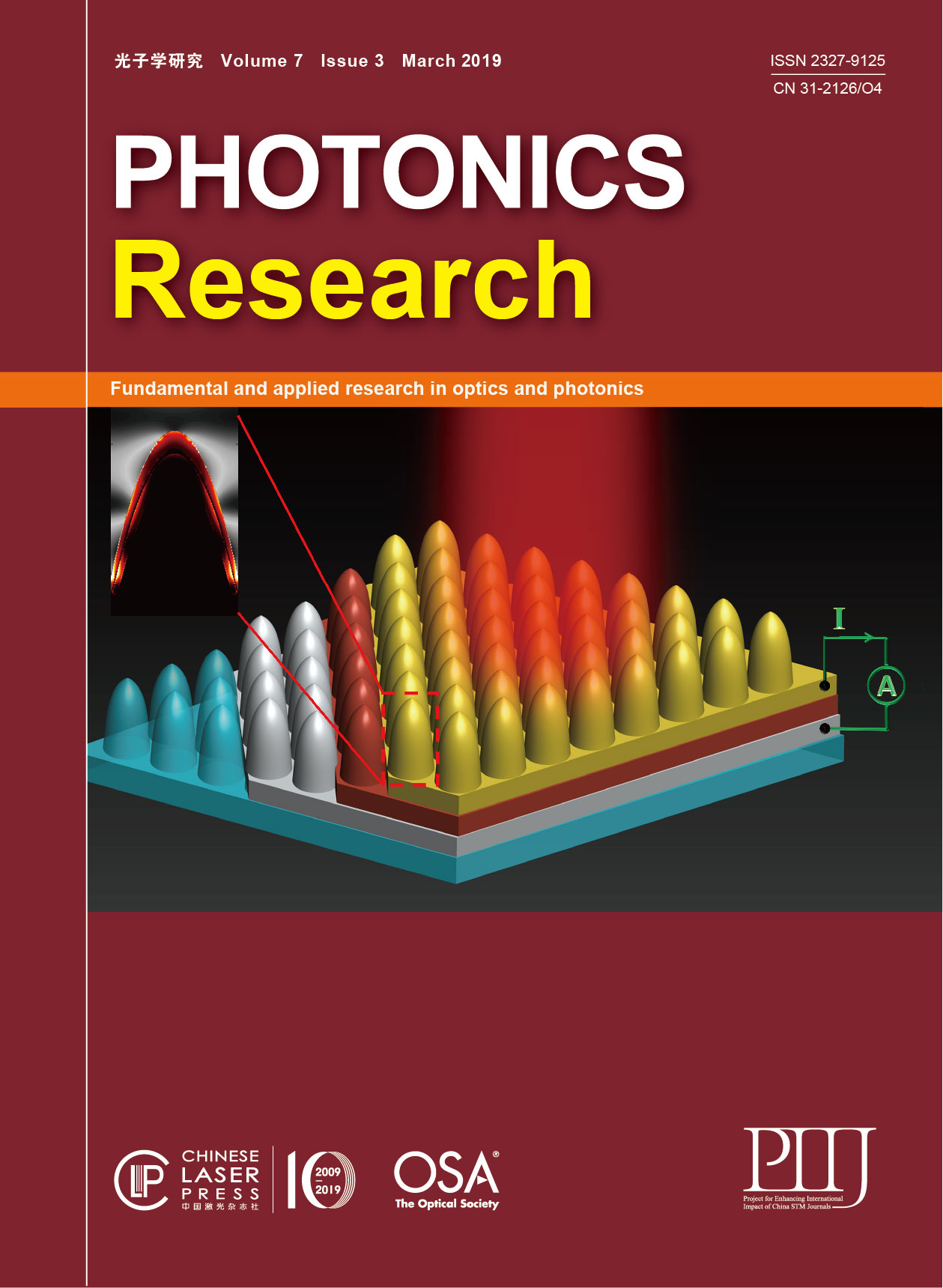
The schematic of the optical switch based on SHM is depicted in Fig. 1(a). The SHM is constructed by stacking monolayer graphene sheets with surface conductivity and dielectric layers with permittivity alternatively along the axis with a period . is adopted to be 2.2, which was used in Ref. [25]. The SHM and air are above and below the interface, respectively. The SHM is truncated at a slanted angle with respect to the axis.
Fig. 1. (a) Schematic of the zero-reflection-based optical switch; the period of the SHM is . (b), (c) and as functions of frequency and chemical potential.
Graphene is a very thin material layer with a thickness as small as one atom, which is very small compared with the period of the SHM. Moreover, it has extremely high carrier mobility of , which theoretically makes an optical switch with high response speed on the order of possible [42]. In our study, graphene is modeled as a two-dimensional surface and characterized by using a surface conductivity rather than a volumetric permittivity. The surface conductivity of graphene can be calculated by the Kubo formula [19,43]: where is the charge of an electron, is the Boltzmann’s constant, is the reduced Planck constant, is the Fermi–Dirac distribution, is the energy, is the frequency, and is the chemical potential determined by the carrier density . is the phenomenological scattering rate. is the temperature. The above surface conductivity material function is available in the material database in finite-difference time-domain (FDTD) software.
To realize the optical switch to be discussed later, the chemical potential of all graphene sheets needs to be changed simultaneously. The chemical potential depends on the carrier density and can be controlled by its chemical potential, external electrostatic field biasing, gate voltage, magnetic field, chemical doping, or nonlinear effect [19–22" target="_self" style="display: inline;">–22]. For example, one effective way to do this is by using external electrostatic field biasing . The relation between and is deduced as [18,19]where is the Fermi velocity, and is the permittivity of free space. The other parameters are the same as those in Eq. (1).
In the THz spectrum, the period of the structure is far less than the working wavelength. So the designed SHM can be modeled as a homogenous uniaxial anisotropic medium by the effective medium approximation method. The diagonal elements of effective relative permittivity tensor of the SHM is described as and given as follows [44]: where and denote the components parallel and perpendicular to the graphene sheets.
From Eq. (3), one knows that is a constant equal to the permittivity of dielectric layers, while is complex, depending on frequency and chemical potential . By combining Eqs. (1) and (3), and are calculated and shown in Figs. 1(b) and 1(c). In Fig. 1(b), one can see that decreases as increases or decreases. Moreover, the value of can cross the threshold of zero by tuning in a wide frequency range. In Fig. 1(c), one can see that is small enough to be neglected as compared with when .
2.2 B. Realization of the All-Angle Zero-Reflection-Based Optical Switch
As depicted in Fig. 1(a), a Gaussian beam with waist width of 10 μm is incident from the SHM to air at an incident angle . Due to the symmetry of the 1D periodic structure, only the – section needs to be considered. The simplified dispersion relation of extraordinary waves (TM waves) is given as where is the wavenumber in vacuum. is positive and cannot be tuned after fabrication. is a complex number depending on and . However, Figs. 1(b) and 1(c) imply that is approximate to a real number due to its tiny when . The IFC is an ellipse with , while it will become a hyperbola with .
To reveal the principle of the zero-reflection-based optical switch, we consider the conditions of and . For the OFF-state, an elliptic IFC is required, i.e., . Figures 1(b) and 1(c) suggest that decreases from positive to negative as increases, and is sufficiently small to be neglected when . Therefore, we take for the OFF-state. For simplicity, we will use instead of in the following study unless there are additional specifications. As for the ON-state, the zero-reflection-based optical switch requires a hyperbolic IFC with its asymptote perpendicular to the SHM–air interface. This means that the slope of the asymptote should be and . According to Fig. 1(b), one can get at for the ON-state.
IFC analysis is used to study the propagation behaviors on the SHM–air interface, as shown in Figs. 2(a) and 2(b). For simplicity, and have been normalized by . In Fig. 2(a), the optical switch is switched off when . Obviously, there exist reflected wave vector and energy flow , while there is no refracted wave, since the conservation line [i.e., the red dashed line in Fig. 2(a)] does not intersect with the air IFC. In Fig. 2(b), the optical switch is switched on when . Since the normal of the SHM–air interface is parallel to the asymptote of the hyperbolic IFC, one cannot get the reflected wave vector on the IFC of the SHM. Meanwhile, there is no refracted wave either. In other words, one can realize zero reflection and zero refraction simultaneously at the ON-state.
Fig. 2. IFC analysis and simulation results for the optical switch at and . (a), (c) Switch-off state (). (b), (d) Switch-on state (). The inset shows the enlargement of the energy distribution in the denoted square area.
To verify the above predictions, FDTD simulations for a graphene–dielectric structure with actual parameters are shown in Figs. 2(c) and 2(d), which match well with the analysis in Figs. 2(a) and 2(b). For the ON-state in Fig. 2(d), it is hard to see where the energy goes, since most of it is localized near the incident area at the interface. In order to show the propagation behaviors more clearly, a monitor is introduced to record the evolution of the electromagnetic (EM) wave as time elapses. Figure 3 shows snapshots of the evolution movie of the electric field for a Gaussian beam with a finite length of 4850 time steps recorded by the monitor. Obviously, in the case of no reflection and no refraction, the EM wave changes into a surface wave to propagate in the upper-right direction along the air–SHM interface and escape finally. The enlargement inset in Fig. 2(d) also verifies this point. It should be noticed that in order to efficiently couple the EM wave into the structure, the optical switch is designed to be an isosceles right triangle SHM, as shown in Fig. 1(a). The left SHM–air interface with is used for coupling light into the device. The transmission for the EM wave incident from the left side is as high as 97% at normal incidence, which is high enough for the application of the device.
Fig. 3. Snapshots at different time steps for a Gaussian beam with a finite length of time steps. (a) time steps (before touching the interface), (b) time steps (arriving at the interface), and (c) time steps (stably propagating along the interface). (d)–(f) Three snapshots after the Gaussian beam stops emitting from the source.
It is necessary to discuss the influence of the loss of the dielectric on the optical switch. The loss of the dielectric is characterized by the imaginary part of its permittivity. Figure 4 shows the influence of absorption loss of dielectric layers on the OFF-state () and ON-state (). Obviously, the larger the loss, the faster it decays with increasing distance. However, the loss has almost no essential influence on the propagation characteristics of the EM wave. For example, when , it results in a lower reflection only at the OFF-state, but keeps near-zero reflection at the ON-state. Therefore, for simplicity, we assume that the loss of the dielectric is zero for our study.
Fig. 4. Influence of absorption loss of dielectric layers on the optical switch. (a) OFF-state (). (b) ON-state ().
Further IFC analysis suggests that the optical switch exhibits zero reflection for arbitrary incident angle from 0° to 90° as long as the frequency and chemical potential are maintained. However, the phenomenon of zero refraction is limited by . If decreases continually, a refracted wave vector satisfying the conservation condition will appear on the air IFC. So there exists a critical incident angle to decide whether zero refraction appears or not. For and , is calculated to be 42.3°. However, the refracted light would not disappear completely until in actual FDTD simulations. This is attributed to the width of the waist of the Gaussian light beam. As we know, the smaller the width of the waist, the larger divergence of the Gaussian beam, and thus it results in a wider incident angle range of the Gaussian beam. As for the Gaussian beam with waist width of 10 μm used here, its divergence angle is about 14.4°. Therefore, the refracted light still exists within (i.e., ), but its intensity weakens as increases. It should be mentioned that similar phenomena also occur for other sources, including a plane wave, which has an ideal incident angle.
2.3 C. Influence of Dispersion on the Designed Optical Switch
The influence of dispersion can be studied by calculating the reflection as a function of for frequencies around . The incident power in FDTD simulations is set to be unity. Reflection is defined as the energy flowing through the top and left sides of the structure in Fig. 1(a). For , the curves of reflection versus are shown in Fig. 5. For , the reflection reaches zero exactly at , which agrees well with the IFC analysis in Fig. 2(b). Moreover, the reflection curve shifts rightward as increases; however, the reflection for the OFF-state (or ON-state) at (or 0.82 eV) remains high () (or near-zero) for , 25 THz, and 25.5 THz, meaning that the dispersion of the SHM has almost no influence on the optical switch. What is more, from the viewpoint of applications, such a strict condition for the switch, i.e., single value of chemical potential (0.2/0.82 eV), can be relaxed to a range of chemical potentials, provided that the ratio of reflections at the OFF- and ON-states is high enough. Figure 5 shows that the reflection remains high () and stable within for the OFF-state, and it becomes near zero () within for the ON-state from 24.5 THz to 25.5 THz. The ratio of reflections at the OFF- and ON-states is as high as , which is high enough for application. This implies that the optical switch can work in a frequency range by using combinations of within these two ranges as control parameters, rather than just 0.2/0.82 eV. Such a property provides high tolerance of chemical potential for the optical switch and makes it very convenient in practical applications.
Fig. 5. Variation of reflection with chemical potential for , 25 THz, and 25.5 THz.
3.1 A. Influence of the Permittivity of Dielectric Sheets and the Period of the Structure
In previous studies, we made default assumptions of and . Actually, these two parameters can efficiently adjust the working frequency range () of the optical switch. From the discussion in Section 2.B, one can get that for , the condition of the optical switch is that should be tuned to guarantee (for the OFF-state) or (for the ON-state). Actually, is affected not only by but also by . In other words, the working frequency range () can be determined by and together.
First, we discuss the lower limit . Figures 1(b) and 1(c) show that increases with decreasing ; however, increases rapidly when decreases from 0.2 eV to 0 eV, so is the minimum available value. On the other hand, decreases from positive to negative as decreases. Obviously, there exists a frequency threshold where [or for simplicity due to negligible ]. Since the OFF-state requires , this frequency threshold is . In a word, is determined by and together. As for , Fig. 1(b) shows that with increasing increases, and a larger is required to maintain for the ON-state. However, cannot increase indefinitely. So we assume to be the maximum available value, since in this case, the reflection is still near zero as discussed in Section 2.C. Therefore, is determined by and .
It is convenient to obtain and from the curves to study the influence of and . We first study the influence of while keeping . The relations of versus satisfying and for different are presented in Figs. 6(a) and 6(b), respectively. and are determined by the intersections of curves and the two dashed horizontal lines located at and 0.9 eV, respectively. Obviously, both and decrease as increases, and the absolute bandwidth decreases, too. In other words, the smaller the , the wider the bandwidth. Specifically, the working frequency ranges, i.e., (), are (24.8, 38.7) THz, (17.1, 26.1) THz, (14.8, 22.4) THz, (12.7, 19.3) THz, and (11.5, 17.3) THz for , 2.2, 3, 4, and 5, respectively. For the designed optical switch with and in Section 2, it can work in a broad frequency range from 17.1 THz to 26.2 THz.
Fig. 6. curves with different parameter conditions: (a) , ; (b) , ; (c) , ; (d) , . The dashed lines indicate and 0.9 eV, respectively.
Then we study the influence of while keeping as a constant. Without loss of generality, we keep , though it is impossible to select air () to construct a real SHM. Figures 6(c) and 6(d) show the curves satisfying conditions of and , respectively, for different . Through similar analysis, one can find that no matter whether or , all curves shift rightward as decreases, meaning that both and increase with decreasing . Specifically, the working frequency ranges are (48.2, 85.4) THz, (31.2, 49.7) THz, (24.8, 38.7) THz, (21.6, 32.7) THz, and (19.1, 28.9) THz for , 0.06 μm, 0.1 μm, 0.14 μm, and 0.18 μm, respectively. Apparently, the absolute bandwidth decreases significantly as increases (from 37.2 THz to 9.8 THz when increases from 0.02 μm to 0.18 μm).
3.2 B. Influence of the Slanted Angle α on the Zero Reflection Effect
So far, we have assumed . Actually, no matter what is, it is always possible to realize zero reflection provided that the asymptote of the hyperbolic IFC is perpendicular to the interface whose slope is . For the hyperbola described by Eq. (4), the slope of one asymptote is . So we get the required described by from as For parameters of and , the required for zero reflection are , , , and when , and 80°, respectively. For these special values of , the relations of versus are shown in Fig. 7(a), which can be used to determine the upper limit . When increases, the corresponding curve shifts rightward, leading to a larger . The upper limits for , and 80° are 12.6 THz, 26.2 THz, 32 THz, and 36.3 THz, respectively, as denoted by the dashed line at in Fig. 7(a). On the other hand, since the required for OFF-state still remains at 0.2 eV, the lower limit is still 17.1 THz. Therefore, it is an effective way to enlarge the working bandwidth by increasing the slanted angle .
Fig. 7. (a) curves for , 45°, 60°, and 80°. (b) IFC at for and . (c) Dependence of maximal incident angle on the slanted angle .
We further discuss the effective incident angle range (). One asymptote of the hyperbolic IFC perpendicular to the SHM–air interface has a slope of . The SHM supports wave vectors only within these two asymptotes, as shown in Fig. 7(b) where the hyperbolic IFC at for the case of and is drawn. Obviously, is 0°. As for , if the angle between the two asymptotes is less than 90°, ; otherwise, because an incident angle cannot be larger than 90°. The curve of versus is shown in Fig. 7(c). Obviously, decreases linearly when . Usually, is desired to be as large as possible, and at the same time the SHM should support arbitrary between 0° and 90°. Therefore, is the optimal selection for the SHM–air interface.
4. CONCLUSION
In conclusion, we have realized the zero reflection effect in a graphene–dielectric SHM and demonstrated an all-angle compact optical switch. The IFC of this SHM can be conveniently switched between an ellipse and a hyperbola by tuning the chemical potential. In particular, when the asymptote of the hyperbolic IFC is perpendicular to the SHM–air interface, zero reflection can be realized. Based on these unique properties, an all-angle optical switch is proposed. It can work at high reflection () (OFF-state) over and near-zero reflection (ON-state) over , providing high tolerance of chemical potential in practical applications. Moreover, its working bandwidth can be effectively adjusted by permittivity of the dielectric, period of the structure, and the slanted angle of the SHM–air interface. These results hold great potential in many fields, such as data storage, beam steering, and THz wave sensing, as well as integrated photonic circuits.
 Download: 621次
 Schematic of the zero-reflection-based optical switch; the period of the SHM is d. (b), (c) Re(ε‖) and Im(ε‖) as functions of frequency and chemical potential.")
, (c) Switch-off state (μc=0.2 eV). (b), (d) Switch-on state (μc=0.82 eV). The inset shows the enlargement of the energy distribution in the denoted square area.")
 ts=100 time steps (before touching the interface), (b) ts=200 time steps (arriving at the interface), and (c) ts=2000 time steps (stably propagating along the interface). (d)–(f) Three snapshots after the Gaussian beam stops emitting from the source.")
 OFF-state (μc=0.2 eV). (b) ON-state (μc=0.82 eV).")

 ε‖=0, d=0.1 μm; (b) ε‖=−εd, d=0.1 μm; (c) ε‖=0, εd=1; (d) ε‖=−1, εd=1. The dashed lines indicate μc=0.2 eV and 0.9 eV, respectively.")
 μc-f curves for α=20°, 45°, 60°, and 80°. (b) IFC at f=25 THz for α=80° and ε‖=−0.07. (c) Dependence of maximal incident angle θimax on the slanted angle α.")


 PDF全文
PDF全文

