Photonics Research, 2018, 6 (4): 04000277, Published Online: Aug. 1, 2018
Ultra-compact and broadband electro-absorption modulator using an epsilon-near-zero conductive oxide  Download: 507次
Figures & Tables
Fig. 1. (a) 3D Schematic of the plasmonic EA modulator. (b) Enlarged view of the cross-sectional area of the active E-O modulation region and (c) enlarged view of the Au slot waveguide with tapers to silicon waveguides.
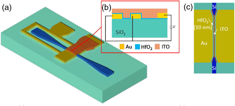
Fig. 2. Simulated optical mode profiles for (a) the plasmonic slot waveguide with N p = N b = 1 × 10 20 cm − 3 N p = 7.5 × 10 20 cm − 3 N b = N p = 1 × 10 20 cm − 3 N p = 7.5 × 10 20 cm − 3

Fig. 3. (a) Optical image of the plasmonic slot waveguide integrated with Si waveguides. (b) SEM image of the plasmonic slot waveguide. (c) Enlarged SEM image of the tapered region. (d) SEM image of the cross-sectional view of the slot waveguide.

Fig. 4. (a) Change of the measured (blue) and simulated (red) transmission with the applied gate voltage. (b) Left: measured static transmission spectra with no applied bias and 3.5 V bias. Right: measured ER with 3.5 V applied bias.


Qian Gao, Erwen Li, Alan X. Wang. Ultra-compact and broadband electro-absorption modulator using an epsilon-near-zero conductive oxide[J]. Photonics Research, 2018, 6(4): 04000277.


 PDF全文
PDF全文

