1. INTRODUCTION
Electro-optic (E-O) modulators are key components in optical communication systems and play critical roles for future data centers and clouds. To meet the exponentially increasing demands of bandwidths and stringent challenges in energy consumption, E-O modulators should offer a compact size and high energy efficiency, as well as a broad operational bandwidth across the telecommunication wavelength window to enable wavelength division multiplexing (WDM) [1]. Existing E-O modulators are based on either resonators such as micro-rings [2,3] and photonic crystal micro-cavities [4,5] or non-resonant broadband devices such as Mach–Zehnder interferometers [6,7] and electro-absorption (EA) modulators [8]. Resonators can achieve high energy efficiency; however, they also suffer from limited bandwidth and require complex control of temperature and high fabrication precision to operate at the desired wavelengths. In contrast, non-resonant modulators offer a large operational wavelength range and can be used in WDM systems to increase the overall bandwidth. Compared with resonators, however, a much longer modulation length is required to achieve sufficient phase shift or electrically induced optical absorption using similar driving voltage for non-resonator modulators. Meanwhile, a large device length also induces a large capacitance, which can increase the resistance–capacitance (RC) delay and induce high energy consumption.
Transparent conductive oxides (TCOs) are wide bandgap semiconductors with a large tunability of optical permittivity by their free carrier concentration, which is described by the Drude model [9]. The optical properties of TCOs can be changed from dielectric-like to metallic-like using a gate voltage. During the transition, the absolute permittivity will reach a minimum value and TCOs become epsilon-near-zero (ENZ) materials [10]. Light will concentrate in the ENZ TCO due to the electric displacement continuity at the interface, thus further enhancing light–matter interaction. In recent years, a new type of TCO-based plasmonic EA modulators has been reported both in theory [1113" target="_self" style="display: inline;">–13] and experimentally [1416" target="_self" style="display: inline;">–16]. The ENZ effect that results from the dramatic change of free carrier concentration in TCO materials provides an unprecedented capability to absorb light over a broad wavelength range, which makes EA modulators ultra-compact as well as broadband. In addition, TCO materials are fully compatible with silicon photonics and can be readily integrated with existing photonic integrated circuits (PICs). In this paper, we present an ultra-compact, broadband gold (Au) plasmonic slot waveguide EA modulator using electrically controlled indium-tin oxide (ITO) that can reach ENZ with a moderate gate voltage. The device is fabricated on a commercial silicon-on-insulator (SOI) wafer by coupling two standard silicon waveguides with a 3 μm long, 300 nm wide Au slot waveguide. In the active E-O modulation region, a metal-oxide-semiconductor (MOS) capacitor is used to electrically switch the ITO into ENZ. We first provide a brief overview of the modulator design, including its architecture and operating principles. In particular, we will simulate how the accumulated free electrons in the ITO layer will induce optical absorption under the applied bias voltage. Then we will present the fabrication process and characterization of the device, including both static and dynamic E-O modulation. We then conclude this paper with a discussion of the modulator’s performance for future optical interconnect systems in terms of modulation bandwidth and energy efficiency.
2. DEVICE DESIGN
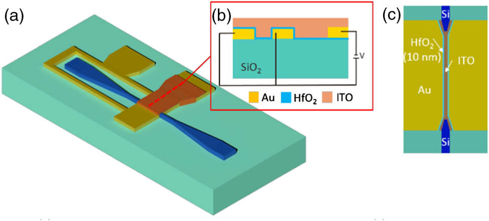
The 3D schematic of the plasmonic EA modulator is shown in Fig. 1(a) and is designed on a standard SOI wafer. The device consists of an active Au plasmonic slot waveguide with electrodes between two silicon waveguides. Two grating couplers are used to couple light into and out of the Si waveguides [17]. The designed grating couplers can be patterned along with the silicon waveguide through the same electron beam lithography (EBL) and etching process, which reduces fabrication complexity. This reported transverse electric (TE)-polarized subwavelength grating coupler has 3 dB bandwidth of 52 nm from our simulation. A pair of Si–Au tapers, as shown in Fig. 1(c), performs the Si strip waveguide to plasmonic slot waveguide mode conversion [18]. Briefly, the evanescent field of the silicon waveguide will first excite the surface plasmon polariton (SPP) mode at the metal–dielectric interfaces and then gradually evolve into the mode of the ITO-filled metal–insulator–metal (MIM) waveguide [19,20]. The Au tapers have a small angle of 9° to ensure a quasi-adiabatic transition with conversion efficiency of 70% [18]. The plasmonic slot waveguide, which is also the active E-O modulation region, is made up of two Au slabs with a 300 nm slot, as shown in Fig. 1(c). 10 nm thick is deposited on top of the Au slot waveguide, followed by filling the slot with 200 nm thick ITO. Another Au slab is deposited on top of the layer to serve as the connecting electrode with the ITO layer. The cross-sectional view of the /ITO film stack, which creates an MOS capacitor, is shown in Fig. 1(b). The Au slot waveguide and the top ITO are connected to two Au electrodes to apply a bias voltage across the MOS structure. If a negative bias is applied at the gate (ITO), it will cause up-bending of the conduction band of the ITO; therefore, an accumulation layer of free electrons will be formed in the ITO layer at the interface. The accumulation layer will induce strong perturbation to the complex permittivity of the ITO layer by reducing the real part and increasing the imaginary part. When the ITO reaches the ENZ region, strong electrically induced absorption will occur due to the interaction between the SPP mode and the accumulation layer.
Fig. 1. (a) 3D Schematic of the plasmonic EA modulator. (b) Enlarged view of the cross-sectional area of the active E-O modulation region and (c) enlarged view of the Au slot waveguide with tapers to silicon waveguides.
下载图片 查看所有图片
The electrically induced absorption was simulated by finite-difference time-domain (FDTD) method of Lumerical Solutions. The optical properties of the ITO are described by the well-established Drude model [9]. The relative permittivity, , is given by , where is the high-frequency dielectric constant, is the plasma frequency defined as , and is the plasma collision frequency. Here, is the free carrier concentration, is the electron charge, is the vacuum permittivity, and is the effective mass of the carrier. The plasma collision frequency is related with the carrier mobility by . In our simulation, the bulk carrier concentration is , which was measured by the Hall effect. We also simulated the eigenmodes of the Au slot waveguide filled with 10 nm and 200 nm ITO, from which the propagation loss can be calculated from the imaginary part of the effective index. When no bias voltage is applied and we assume the free carrier concentration is for the entire ITO layer, the optical field distribution of the Au slot waveguide mode is shown in Fig. 2(a), and the waveguide loss is 0.58 dB/μm. We designate this relatively low loss state as the “ON state.” By applying a negative bias on the ITO gate layer, electrons accumulate at the interface, resulting in an increase of the imaginary part of the permittivity. To simplify the analysis, we consider the carrier accumulation process by adding an effective accumulation layer at the interface in the simulation with uniform carrier concentration . The thickness of the accumulation layer is usually estimated by the Thomas–Fermi screening length, which is estimated to be around 1 nm [21]. As the bias voltage becomes more negative, the imaginary part of the ITO refractive index becomes larger and the light absorption is prominent. When the carrier density of the accumulation layer is , which switches the accumulation layer of ITO into ENZ, the EA is the strongest and we define it as the “OFF state.” The optical field distribution of the Au slot waveguide mode at the OFF state is shown in Fig. 2(b) and the waveguide loss is 3.20 dB/μm, which indicates a 2.62 dB/μm modulation strength. It is interesting to point out that the optical field is concentrated in the ENZ layer due to the continuity requirement of the electric displacement [10]. We further performed a 3D optical transmission simulation by modifying the ITO material index parameters for both the ON () and OFF ( and ) states. In the simulation, we launched a mode-matched light beam from the left into the couple-in silicon waveguide and monitored the power flow through the couple-out silicon waveguide on the right, as shown in Figs. 2(c) and 2(d). We also calculated the propagation loss as a function of the peak carrier concentration in the accumulation layer of ITO film, as shown in Fig. 2(e). There is a sharp increase of the light absorption when the ITO approaches ENZ, while the EA below increases quite slowly, which agrees with Vasudev et al.’s analysis [11]. Figure 2(f) shows the optical transmission spectra at the ON state and OFF state. A big extinction ratio () at 1.55 μm can be observed due to the ENZ ITO absorption. Since the ENZ effect is due to the plasmon resonance, which requires the real part of the optical permittivity of ITO to be close to zero, the bandwidth is limited. In our simulation, the 3 dB bandwidth is 70 nm, as shown by the red curve in Fig. 2(f).
Fig. 2. Simulated optical mode profiles for (a) the plasmonic slot waveguide with and (b) the plasmonic slot waveguide with ITO at ENZ when . The inset shows the enlarged region with the ENZ ITO layer. Top view of optical field distributions at (c) the ON state (accumulation layer ) and (d) the OFF state (accumulation layer ). The optical field profile is plotted in log scale. (e) The propagation loss of the plasmonic slot waveguide at different peak carrier concentrations. (f) Transmission at the ON state and OFF state and the extinction ratio as a function of the optical wavelength.
下载图片 查看所有图片
3. DEVICE FABRICATION AND CHARACTERIZATION
The Si strip waveguide is fabricated on a commercial SOI wafer with a buried oxide thickness of 3 μm. The Si waveguide is patterned by EBL and reactive ion etching. The Au slot waveguide is first patterned by ZEP e-beam resist with alignment to the Si strip waveguides, followed by thermally evaporating 200 nm thick gold film. Then a lift-off process is used to form the Au slot waveguide with tapers. To realize an active device using a high-efficiency MOS capacitor, a 10 nm was deposited by atomic layer deposition as the gate oxide. Then, the Au slot is filled with 200 nm ITO by sputtering. Both the ITO and the Au slot waveguides (both sides) are connected to a pair of Au electrodes to apply the bias voltage. The optical image of the fabricated device is shown in Fig. 3(a). The scanning electron microscopy (SEM) image in Fig. 3(b) shows the plasmonic slot waveguide with tapers connected to the Si strip waveguides. The zoomed-in SEM image in Fig. 3(c) shows that there is a small alignment error between the Si strip waveguides and the Au slot waveguide, which may induce higher optical loss but will not affect the EA modulation according to our FDTD simulation.
Fig. 3. (a) Optical image of the plasmonic slot waveguide integrated with Si waveguides. (b) SEM image of the plasmonic slot waveguide. (c) Enlarged SEM image of the tapered region. (d) SEM image of the cross-sectional view of the slot waveguide.
下载图片 查看所有图片
We measured the normalized optical transmission of the 3 μm long plasmonic waveguide. The input and output fibers are mounted on two stages with 10° tilted angle that allow precise alignment. A camera is mounted at a 45° angle to visually assist the alignment. The input fiber is a polarization-maintaining fiber with polarization controlled input light (TE mode). The output is collected by a single-mode fiber. The gate voltage is applied between the ITO and Au electrodes through two probes. Figure 4(a) shows the simulated optical transmission of the EA modulator and the experimentally measured results as a function of the applied gate voltage. In simulation, it shows a sharp decrease of the transmission around 3.5 V followed by a rapid increase. The strange phenomenon is caused by approximating the accumulated free carriers as a 1 nm uniform free electron layer, which will cause maximum optical absorption or EA modulation strength at the ENZ transition of ITO in the slot waveguide. In experiment, the electrically induced absorption slowly accelerates as the applied voltage increases, which differs quite significantly from the simulation results in Fig. 4(a) due to the continuous distribution of the accumulated free electrons in real devices. Koch et al. [22] reported the stationary quantum hydrodynamic model to derive the carrier distribution in the accumulation layer upon applying a bias across the capacitor. The calculated continuous carrier distribution is used to compute the modes and the extinction ratio (ER) of the modulator. The results pointed out clearly that uniform accumulation layer approximation would underestimate the ER at higher driving voltage. However, the discrepancy in sub-ENZ modulation requires more investigation. In our experiment, the ER is measured to be 4.5 dB and the corresponding modulation strength is 1.5 dB/μm with 3.5 V gate voltage. We also measured the optical transmission spectra over a broad wavelength range at 0 and 3.5 V bias voltages, as shown in Fig. 4(b). We plotted the ER of the electrically induced absorption modulator in the wavelength range of 1520–1610 nm, which shows a broadband response similar to the simulation results in Fig. 2(f). However, Fig. 2(f) shows a typical Lorentzian resonator limited bandwidth, while our experimental result as shown in Fig. 4(b) has a relatively flat response with 1 dB variation of bandwidth of 70 nm (1530–1600 nm wavelength). Again, we attribute this discrepancy to the uniform accumulation approximation, because the continuous distribution of the free carriers in the ITO layer would homogenize the wavelength response, as well.
Fig. 4. (a) Change of the measured (blue) and simulated (red) transmission with the applied gate voltage. (b) Left: measured static transmission spectra with no applied bias and 3.5 V bias. Right: measured ER with 3.5 V applied bias.
下载图片 查看所有图片
The dynamic modulation speed is demonstrated up to 40 MHz with an AC voltage swing of to 2 V, as shown in Fig. 5, which is limited by our current testing instruments. The signal is applied to the Au bottom electrode layer, and, therefore, a positive/negative bias would cause accumulation/depletion of free electrons in the ITO. As suggested by the simulation, the positive bias will induce accumulated layers of electrons at the interface, resulting in a decrease of transmission. When a negative voltage is applied, the optical transmission will actually increase due to the depletion of free electrons in the ITO layer, but at a smaller scale (30% of the full modulation swing) compared to the drop of transmission (70% of the full modulation swing) under positive gate voltage. This measurement also excluded the possibility of the thermo-optic effect, which usually induces light absorption regardless of the polarity of the gate voltage. We estimated the modulation speed and energy efficiency of the hybrid Si-plasmonic modulator. Since the modulation is based on the accumulation of the MOS capacitor, the speed of the modulator is limited only by the RC delay. The rough estimation of the capacitance of the active region is 15.7 fF. The experimental Hall measurement of the ITO film yields an ON state resistivity of . We calculate the total series resistance of Au and ITO to be around 80 Ω. The RC-limited circuit bandwidth exceeds 250 GHz if we exclude the parasitic capacitance from the contacting pads. We also estimate the energy consumption using , where is the capacitance of the device, and is the applied voltage. With applied voltage of 2.8 V to achieve 3 dB ER, the energy consumption of the device is estimated to be 30 fJ/bit.
Fig. 5. Dynamic optical modulation testing results with to 2 V sweep input bias voltage at 40 MHz.
下载图片 查看所有图片
4. CONCLUSION
In summary, we demonstrated a 3 μm long plasmonic EA modulator on an SOI platform using electrically switched ENZ ITO with an extremely strong modulation of 2.62 and 1.5 dB/μm in theory and experiment, respectively. The EA modulator also experimentally demonstrated a uniform E-O modulation with 70 nm optical bandwidth from 1530 to 1600 nm wavelength and a dynamic E-O modulation speed at 40 MHz. Such ultra-compact, broadband silicon-plasmonic modulators can be used for future WDM on-chip optical interconnects.
5 Acknowledgment
Acknowledgment. This work is supported by the AFOSR under the guidance of Dr. Gernot Pomrenke.
Qian Gao, Erwen Li, Alan X. Wang. Ultra-compact and broadband electro-absorption modulator using an epsilon-near-zero conductive oxide[J]. Photonics Research, 2018, 6(4): 04000277.
 Download: 506次


