1. INTRODUCTION
As a basic component of integrated photonic circuits, an optical waveguide with diverse configurations could confine light propagation within dimensions of micrometer or submicrometer scales, offering a versatile platform for a broad range of applications [1,2]. A few well-developed techniques have been applied to fabricate various waveguide structures in dielectrics, such as ion/proton exchange [3], ion implantation [4], and femtosecond laser writing [5]. Among those developed fabrication techniques, femtosecond laser writing has been widely acknowledged as a powerful 3D micro-processing method to implement versatile photonic structures in a broad variety of materials since the pioneering work lead by Davis et al. in 1996 [6,7]. The focused femtosecond laser pulses can modify the refractive index permanently through a nonlinear process such as multiphoton absorption, avalanche ionization, and tuning ionization [8]. The induced refractive-index modifications could be either positive () or negative (), depending on the laser parameters and physical properties of the processed materials [9,10]. Recently, miniature and integratable laser sources based on the optical waveguide as gain media has attracted great research interest due to the outstanding lasing performances and the ease of integration with other optical devices. Waveguide lasers have been realized in both continuous-wave (CW) and pulsed operation regimes [1113" target="_self" style="display: inline;">–13]. Benefiting from the compact geometry of the waveguide structures, superior lasing performances, e.g., reduced lasing thresholds and enhanced slope efficiencies, could be achieved with respect to the bulk laser systems [14]. Compared with the fiber laser system, the length of a waveguide cavity is much shorter, and the cavity volume is much smaller. The is one of most efficient gain media for solid-state laser systems owing to its outstanding features such as large stimulated emission cross section and strong broadband absorption [15]. For the pulsed laser operation, -switching by saturable absorbers (SAs) inside the laser cavity is one of the most common and efficient methods to generate nanosecond pulses, in which the SAs play an essential role in the ultrafast pulse generation.
In the past few years, graphene and other layered 2D materials, such as transition metal dichalcogenides (TMDCs, e.g., , ), hexagonal boron nitride (-BN), topological insulators (TIs, e.g., ), and black phosphorus (BP) have attracted tremendous interest from fundamental research as well as industries owing to their intriguing properties in a number of aspects [1618" target="_self" style="display: inline;">–18]. Particularly, 2D materials possess unique and distinct optical properties such as polarization-dependent absorption and nonlinear optical absorption, which enable them as promising candidates in photonic applications [19]. Based on the waveguide configuration and nonlinear absorption properties of 2D materials, -switched lasers over a variety of gain media have been widely reported [2022" target="_self" style="display: inline;">–22]. Graphene has been demonstrated to be an ultra-broadband SA with remarkable optical properties such as linear optical absorption and ultrafast recovery time [23]. TMDCs exhibit strong light–matter interaction and ultrafast nonlinear absorption, which enable them as promising candidates for photonic applications [24]. To date, both graphene and have been applied as suitable SA materials in -switched laser systems of waveguides [25,26] and other platforms [27,28]. In addition to the modification techniques implemented to equip desired functionalities of 2D materials [29–32" target="_self" style="display: inline;">–32], the ability to create heterostructures have opened up new possibilities for new physics and unique functionalities by combining distinct 2D materials with diverse properties into van der Waals heterostructures [33]. Monolayer is a direct-bandgap semiconductor with a value of [34] and is therefore a complement to graphene, which is a gapless semimetal. The heterostructure has exhibited superior properties such as tunneling and thermionic transport, weak anti-localization effect, strong spin–orbit interaction, and ultrafast excitation transfer [35–38" target="_self" style="display: inline;">–38]. In optics, the layered heterostructures may introduce new features of SA, resulting in improved performances of lasing [39,40]. In this paper, in an waveguide platform, we implement the passively -switched waveguide lasers based on the SA of heterostructure and compare the lasing characteristics of lasing -switched by separate graphene or SA.
2. EXPERIMENTAL DETAILS AND DISCUSSION
The crystal (doped by 1 at. % ions) used in this work was cut into wafers of dimensions of and was optically polished. The cladding waveguiding structures were fabricated by employing the laser facility of the Universidad de Salamanca, Spain, in which the Ti:sapphire regenerative amplifier (Spitfire, Spectra Physics) was utilized to generate linearly polarized 120 fs pulses at a central wavelength of 800 nm with 1 kHz repetition rate and 1 mJ maximum pulse energy. The pulse energy used to irradiate the sample was reduced by employing a calibrated neutral density filter placed after a half-wave plate and a linear polarizer to better control the incident energy. The sample was placed on a computer-controlled XYZ translation stage. The beam was focused through a microscope objective () at certain depth beneath the largest sample surface (dimensions of 10 mm × 6 mm) at a depth ranges from 140 to 190 μm with a pulse energy of 10 μJ. During the irradiation, the sample was scanned at a constant velocity of 750 μm/s in the direction perpendicular to the laser polarization and the pulse propagation. The scanning direction was carefully aligned with the 10 mm long edge of the sample, thus producing a low refractive-index track along the sample. Under these conditions, the micromachining procedure was repeated at different positions of the sample, forming the desired circular geometry of the cladding waveguide with the diameter of 50 μm.
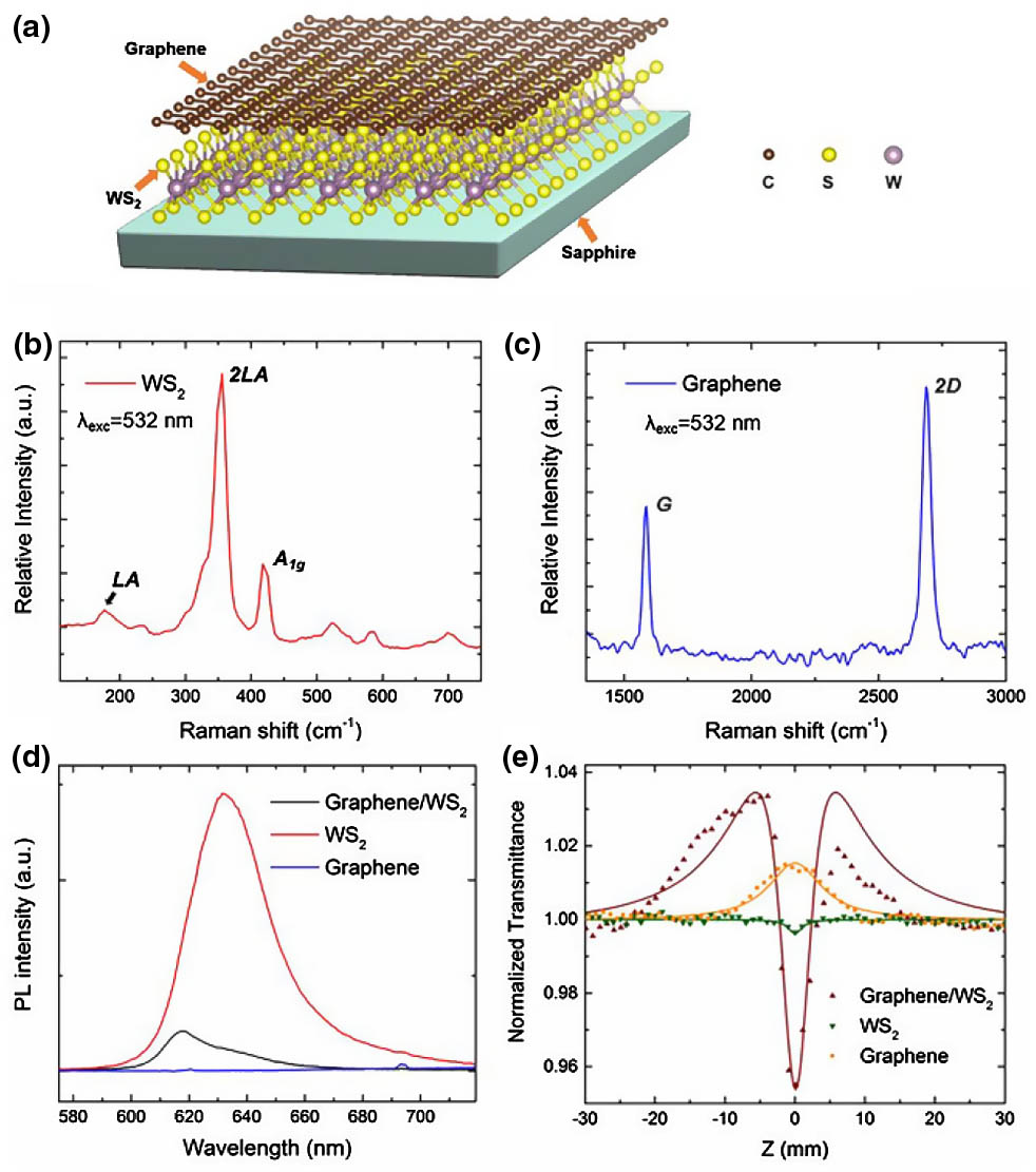
The heterostructure used in this work was synthesized on the sapphire substrate (obtained from 6Carbon Technology). The underlayer was synthesized on sapphire substrate directly via chemical vapor deposition (CVD) growth approach, and the upper-layer graphene was made by CVD and then transferred onto the bottom layer. Figure 1(a) presents a schematic illustration of the vertically stacked heterobilayer of on sapphire substrate. The samples of graphene and used in this work were both fabricated on sapphire substrate by CVD technique and were characterized by Raman spectroscopy, as shown in Fig. 1(b), indicating the monolayer nature and good quality of the two samples compared with previous results [41,42]. Figure 1(d) demonstrates the measured room-temperature photoluminescence (PL) spectrum under the excitation of 532 nm laser in the same conditions. Compared with the PL peak of , a blueshift of the heterostructure has been observed, which may be attributed to the released strain during the transfer process. Moreover, the PL intensity was strongly quenched in the heterostructure, indicating the strong interlayer coupling between the two layers [36]. One possible explanation of the reduced PL intensity of the heterostructure is the ultrafast charge transfer process from to the graphene, which hinders the recombination of photoexcited electron-hole pairs. To further evaluate the optical properties, the nonlinear optical performances of the three samples were investigated through the open-aperture -scan technique under 340 fs pulses operating at 1030 nm with the repetition of 100 Hz in the same configuration [43]. During the -scan experiments, the incident and transmitted powers were measured by two photodetectors, as the samples gradually moved along the laser propagation direction. Figure 1(e) shows the measured normalized transmission of three samples corresponding to the irradiance of at . It is worth noting that the linear absorption and thickness of the as-prepared heterostructure (), (0.8 nm), and graphene (0.4 nm) also have been taken into account in the calculation by employing the UV-Vis spectrophotometer and atomic force microscopy, in which the heterostructure exhibited an enhanced linear absorption. By fitting the -scan data using the nonlinear absorption model [44,45], the heterostructure exhibited stronger nonlinear optical response with the combination of saturable absorption and multiphoton absorption. The fitted saturable intensity of heterostructure was and the nonlinear absorption coefficient () is measured to be , which is much higher than of , which is within a reasonable range under the same condition [43].
Fig. 1. (a) Schematic of heterostructure on sapphire substrate. (b) Raman spectrum of the sample. (c) Raman spectra of monolayer graphene. (d) PL spectrum measured from heterostructure, , and graphene excited by 532 nm solid-state laser at room temperature. (e) Typical open-aperture -scan curves with normalized transmission as a function of sample position .
下载图片 查看所有图片
The -switched waveguide laser experiments were carried out utilizing the end-face coupling arrangement, as illustrated in Fig. 2. A linearly polarized light beam at 808 nm generated from a tunable CW Ti:sapphire laser (coherent MBR-PE) has been employed as the pump source and was set to be TE polarized by placing a linear polarizer. The pump laser was then coupled into the waveguide using a spherical convex lens with a focal length of 30 mm. The radius of the incident pump laser beam is approximately 0.75 nm. An input mirror (with the transmission of 98% at and the reflectivity at ) and SA mirror (SAM) were adhered to the input and output end face of the waveguide, respectively, constructing the Fabry–Perot resonator with the waveguide gain media. The inset of Fig. 2 is the optical image of heterostructure sample used in this work. The generated waveguide lasers were collected by utilizing a microscope objective lens () and detected by an infrared CCD and an oscilloscope. A spectrometer with resolution of 0.2 nm was used to analyze the emission spectra of the pulsed laser beam from the waveguide.
Fig. 2. Schematic of the experimental setup for -switched waveguide laser. Inset is an optical photograph of the heterostructure on sapphire substrate.
下载图片 查看所有图片
In the laser system based on heterostructure SA, the -switched laser emission spectrum from crystalline waveguide is depicted in Fig. 3(a). The central wavelength is 1064 nm with the FWHM bandwidth of , which corresponds to the main emission line of ion transition band to transition. As for and graphene SAs, the same laser emission spectra have been achieved. The inset picture in Fig. 3(a) presents the -switched pulse laser trains under the pumping power of 0.53 W, with the average output power of 104 mW. Figure 3(b) depicts the measured average output power as a function of pumping power through linear fitting. As the increase of launched power, the output power of pulsed laser modulated by SAs of heterostructure, , and graphene climbed to the maximums at 275, 184, and 231 mW with launched pump power of 747, 751, and 715 mW, corresponding to the slope efficiency of 37%, 17%, and 23%, respectively. Meanwhile, by linear fitting, the thresholds of the launched power of the pulsed laser oscillation were calculated to be 57.4, 18.1, and 33.2 mW, respectively. Compared with and graphene, a -switched laser based on SAs of heterostructure has much higher slope efficiency, which demonstrates the enhanced optical performance of this heterobilayer. The insert of Fig. 3(b) presents the measured near-field modal profile evolution of the pulsed laser oscillation as the increase of launched power when the SA is heterostructure, in which the fundamental mode was achieved.
Fig. 3. Efficient -switched waveguide laser emission. (a) Emission spectrum of -switched waveguide laser modulated by heterostructure. Insert is the pulse trains of -switched pulsed laser. (b) Output power versus the launched power. Inset is the evolution of measured near-field modal profile of the -based pulsed laser as the increase of launched power.
下载图片 查看所有图片
Figure 4 illustrates the dependence of pulse parameters (e.g., repetition rate, pulse duration, pulse energy, peak power) based on SAs of heterostructure, , and graphene as a function of launched power in the same conditions. With the increase of the pump power, the repetition rate was tunable ranging from 3.528 to 7.777 MHz, 5.232 to 11.442 MHz, and 2.315 to 8.897 MHz, respectively. Simultaneously, the maximum single pulse energy reached 33.1 nJ ( heterostructure), 16.1 nJ (), and 26.0 nJ (graphene). By using heterostructure as SA, the FWHM of the output laser was 149 ns and then rapidly decreased into a stable value of 66 ns. Moreover, the peak power ranges from 46.5 to 500.9 mW. Compared with and graphene, a -switched laser based on SA of heterostructure has superb performances with relatively higher pulse energy and peak power.
Fig. 4. Comparison of the parameters of pulsed laser -switched by SAs of graphene/WS heterostructure, , and graphene. (a) Repetition rate and pulse duration as a function of launched power. (b) Pulse energy and peak power as a function of launched power.
下载图片 查看所有图片
3. CONCLUSIONS
In conclusion, we have fabricated a cladding waveguide structure in the crystal and realized efficient passively -switched waveguide lasers modulated by using novel heterostructure as an SA. The maximum output power was measured to be more than 275 mW with slope efficiency of 37%, corresponding to a single pulse energy of 33.1 nJ, of which higher pulse energy and enhanced slope efficiency were achieved by the comparison of and graphene under the same configuration. The substrate effects of 2D layers with a different stacking sequence could be carried out in the future works. This work indicates that the layered heterostructure could serve as promising SA materials for ultrafast photonic applications.
Ziqi Li, Chen Cheng, Ningning Dong, Carolina Romero, Qingming Lu, Jun Wang, Javier Rodríguez Vázquez de Aldana, Yang Tan, Feng Chen. Q-switching of waveguide lasers based on graphene/WS2 van der Waals heterostructure[J]. Photonics Research, 2017, 5(5): 05000406.
 Download: 1009次


