中国激光, 2019, 46 (10): 1000001, 网络出版: 2019-10-25
飞秒激光直写技术制备功能化微流控芯片研究进展  下载: 2898次
Research Progress on Fabrication of Functional Microfluidic Chips Using Femtosecond Laser Direct Writing Technology
图 & 表
图 1. TPP加工示意图。(a) TPA工艺;(b) TPP制备方案;(c)实现亚衍射极限(SDL)加工精度的说明,其中单光子吸收(SPA)和TPA的吸收概率分别用虚线和实线表示,插图是衍射图样
Fig. 1. Schematicsof TPP processing. (a) TPA processing; (b) scheme of TPP fabrication; (c) illustration of achievement of sub-diffraction-limit (SDL) fabrication accuracy, in which absorption probabilities for single photon absorption (SPA) and TPA are denoted by dashed and solid lines, respectively, and inset is diffraction pattern
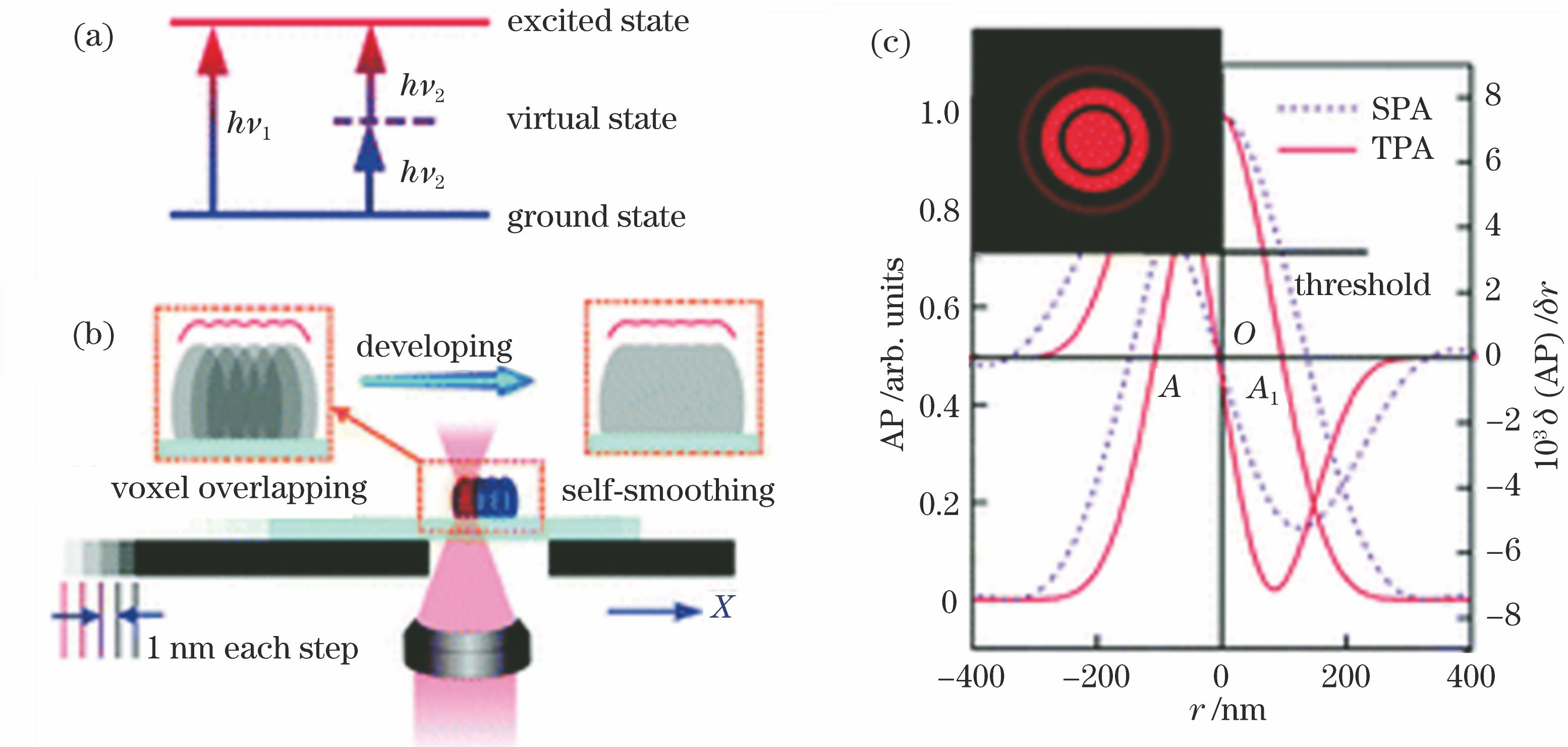
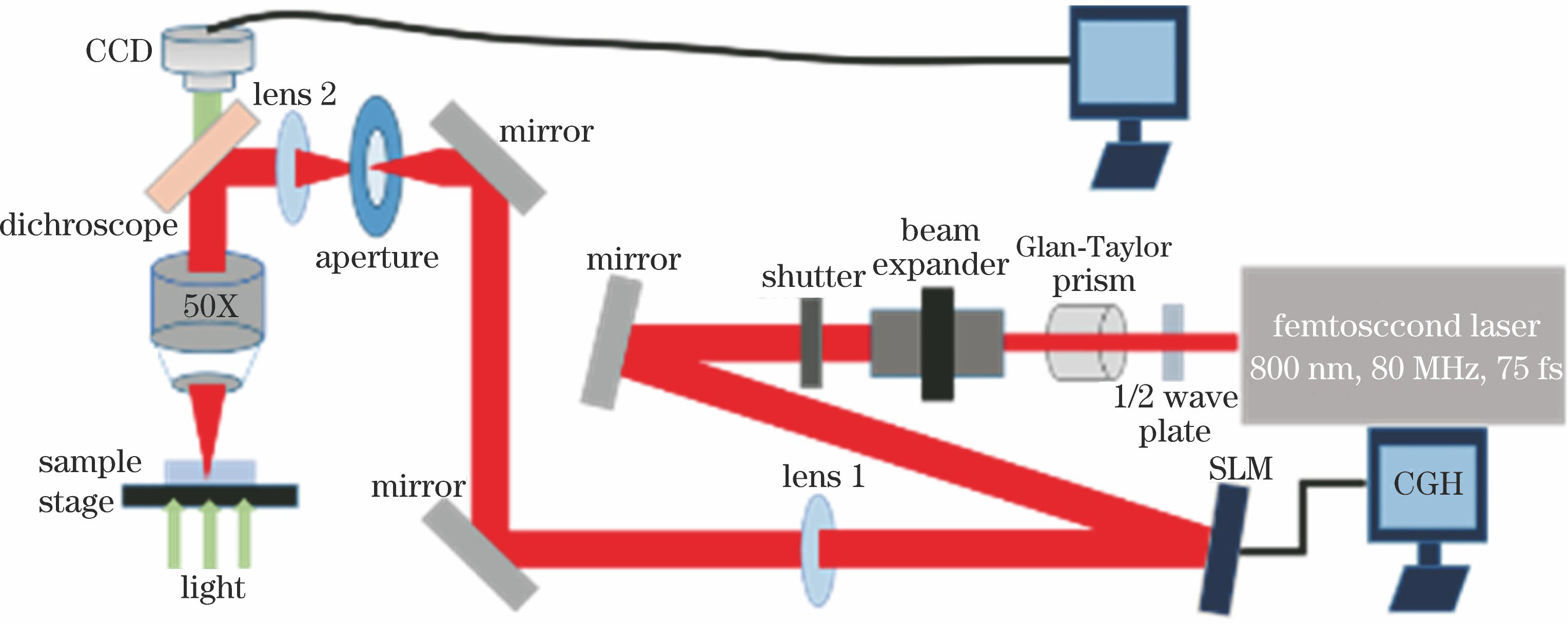
图 3. 玻璃管道中不同的过滤器。(a)不同大小、形状孔的微过滤器的SEM图像;(b)小粒子穿过过滤器的光学显微镜图像;(c)大粒子无法穿过过滤器的光学显微镜图像;(d)单向过滤器SEM图像;(e)、(f)测试单向过滤器的光学显微镜图像
Fig. 3. Different micro-sieves in glass-based microfluidic channel. (a) SEM images of micro-sieves with different pore sizes and shapes; (b) optical microscopic images of sphere with diameter smaller than pore size passing through sieve; (c) optical microscopic images of sphere with diameter larger than pore size not passing through sieve; (d) SEM image of one-way micro-sieve; (e) and (f) optical microscopic images of test of one-way micro-sieve
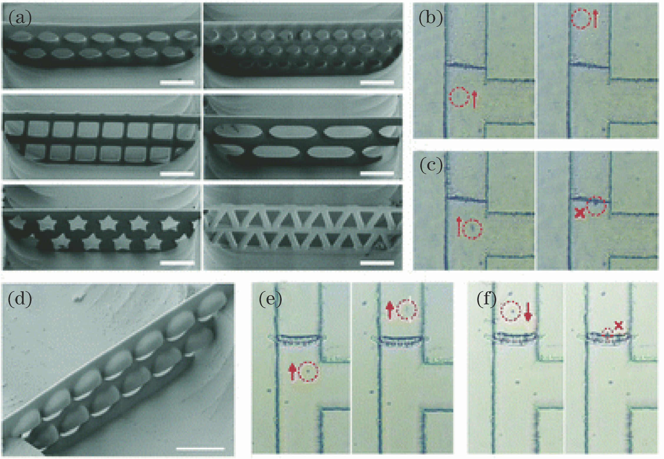
图 4. 不同起始加工位置。低于管道底部的(a)初始位置及(b)相应结构;管道底部下方适当距离的(c)初始位置及(d)相应结构;(e)在光刻胶内部产生的激发荧光;(f)玻璃界面附近产生的激发荧光;(g)玻璃内部产生的激发荧光。图4(e)中的焦点位置比图4(f)中的高3 μm,图4(g)中的比图4(f)中的低3 μm
Fig. 4. Different starting positions of processing. (a) Starting positions lower than channel bottom and (b) resulted structures; (c) starting positions at appropriate distance from channel bottom and (d) resulted structures; (e) foci with strong fluorescence located in photoresist; (g) foci with weak fluorescence located in glass-photoresist interface; (g) foci with weaker fluorescence locate in glass. Position of foci in Fig. 4(e) is 3 μm higher than that in Fig. 4(f) and position of foci in Fig. 4(g)
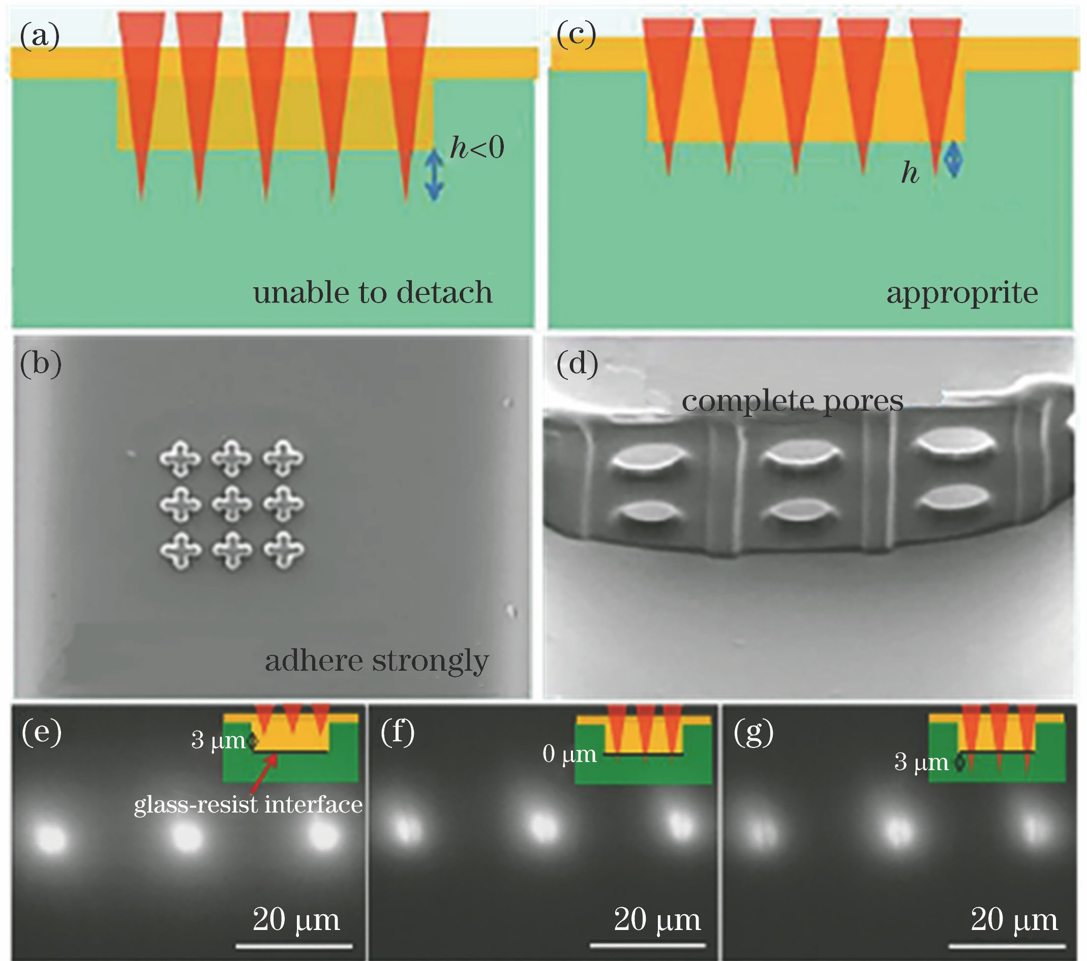
图 5. 实时单粒子捕获。(a)加工系统;(b)捕获粒子的轴侧图;(c)四柱捕获粒子的SEM图像;(d)实时捕获流程:停流、双光子加工捕获粒子、显影;(e)粒子自由运动;(f)八柱捕获示意图和SEM图像;(g)多粒子捕获示意图。比例尺为10 μm
Fig. 5. Real-time single-particle trapping. (a) Processing system; (b) isometric image of trapped particle; (c) SEM image of four-pillar trapping; (d) real-time trapping procedure: stopping flow, two-photon lithography to trap particles, and development to exchange liquid; (e) trapped particles can move freely inside trap; (f) schematic and SEM image of eight-pillar trapping; (g) schematic of multi-particle trapping. Scale bars are all 10 μm
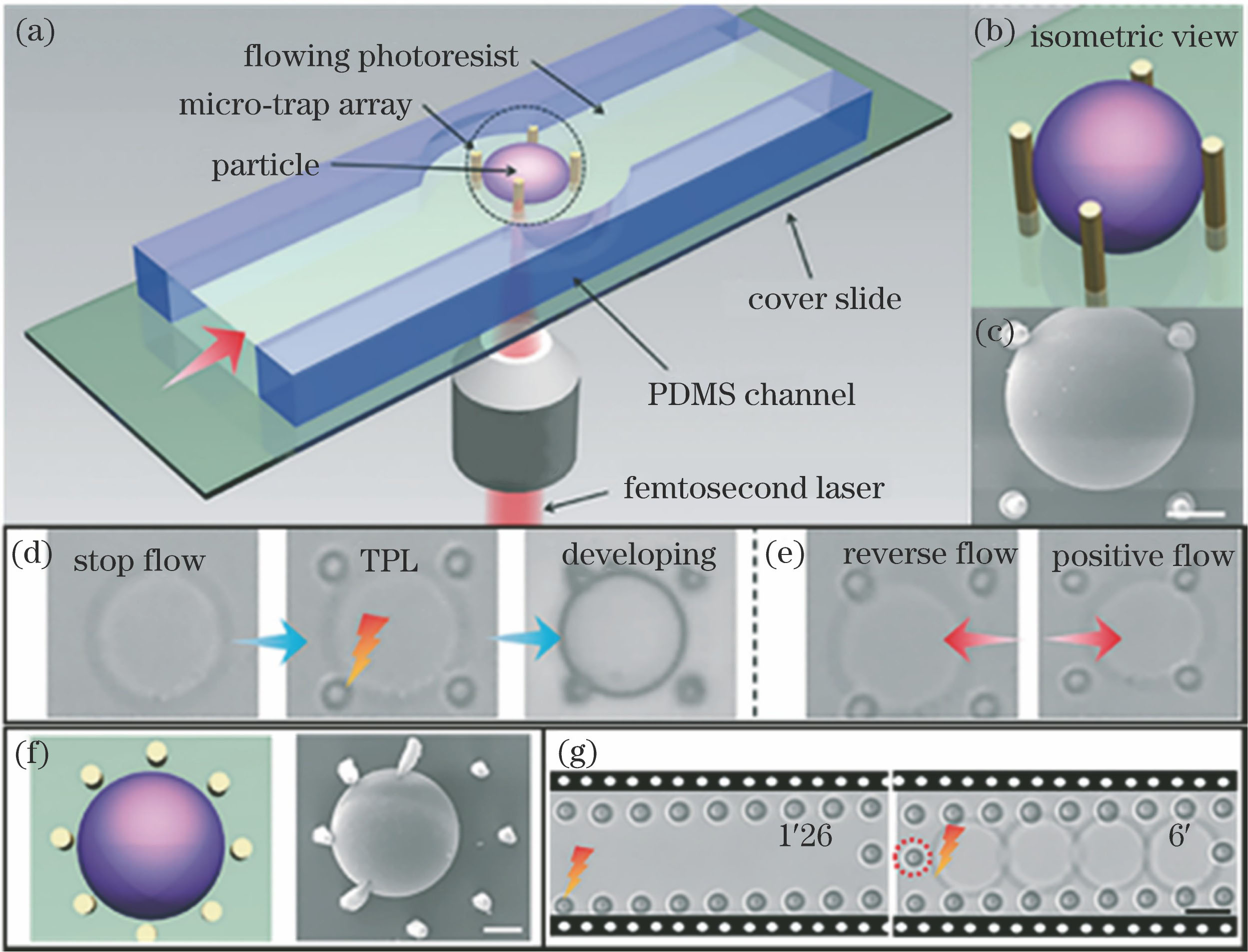
图 6. 螺旋桨微混合器加工示意图。(a)加工系统;(b)微通道设计;(c)直叶片混合器的SEM图像;(d)螺旋形叶片混合器的SEM图像
Fig. 6. Schematics of micromixer with propeller blades. (a) Processing system; (b) Microchannel design; (c) SEM image of micromixer with flat blades; (d) SEM image of micromixer with screw-shaped blades
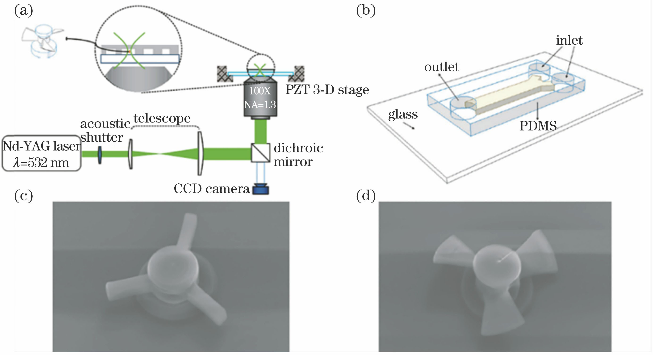
图 7. 拱形微过滤器。(a)大颗粒绕过分选器,中等大小颗粒被捕获在结构中,小颗粒穿过结构示意图;(b)微过滤器的SEM图像;(c)微过滤器的光学显微镜图像;(d)颗粒的分类和收集;(e)粒子分别在入口处、收集处及出口处的光学显微镜图像
Fig. 7. Arch-like microfilter. (a) Schematics of largest particles passing through sorter, median particles being trapped by microfilter, and smallest particles passing through microfilter; (b) SEM image of microfilter; (c) optical microscope image of microfilter; (d) procedure for sorting and collecting particles; (e) optical microscope images of particals introduced into the inlet, the collected targeted-particals and the particals in the outlet, respectively
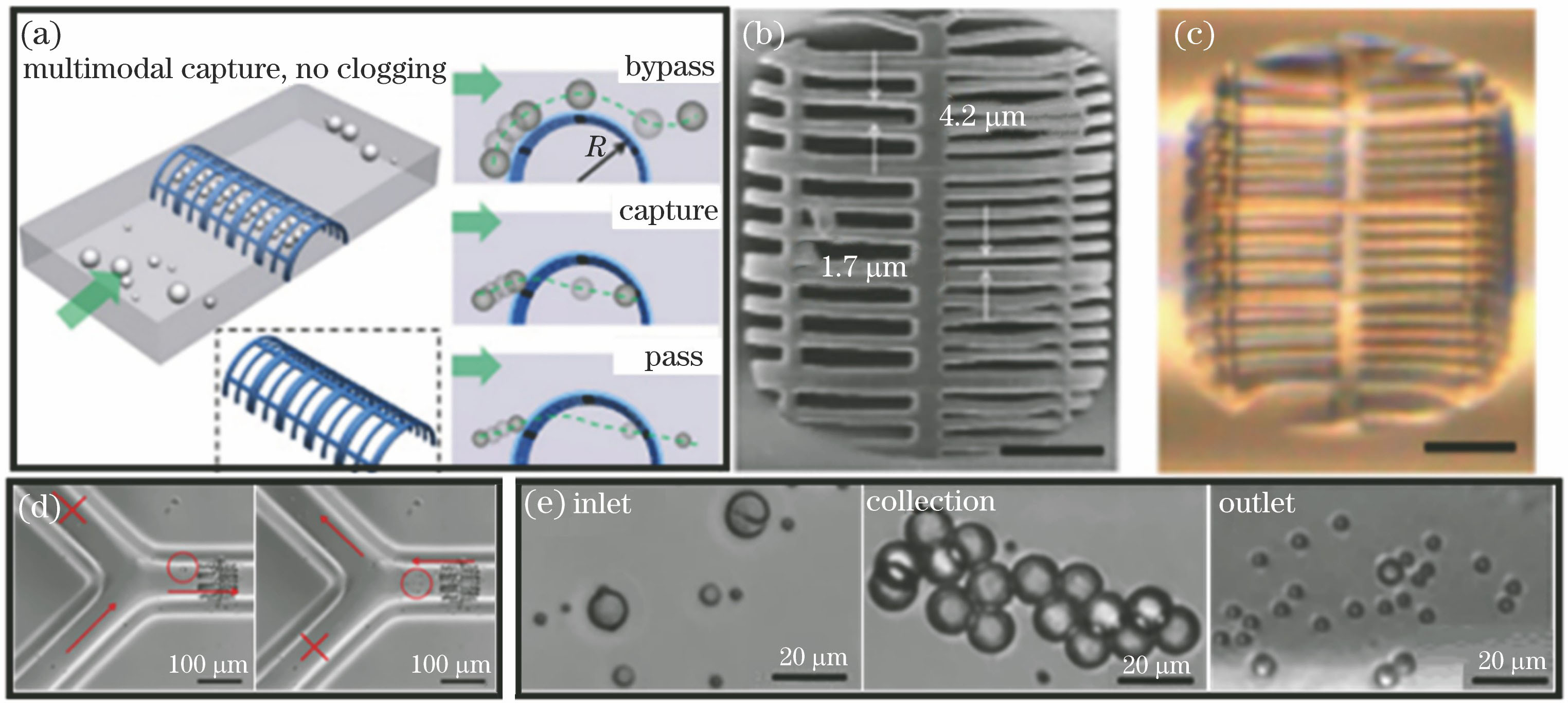
图 8. 交叉流分选器。(a)分选器的结构;(b)分选器中混合粒子(直径分别为5 μm和10 μm)的轨迹仿真;(c)~(f)粒子分选动力学的实验观察(通入溶液10 min后阀1和阀2随时间的形貌变化)
Fig. 8. Cross-flow-based particle sorter. (a) Structure of particle sorter; (b) simulation on trajectories of mixed particles (diameters of 5 μm and 10 μm) in particle sorter; (c)-(f) experimental observation on dynamics of particle sorting (morphologies of sieve I and sieve II changing over time after influx of liquid starting for 10 min)
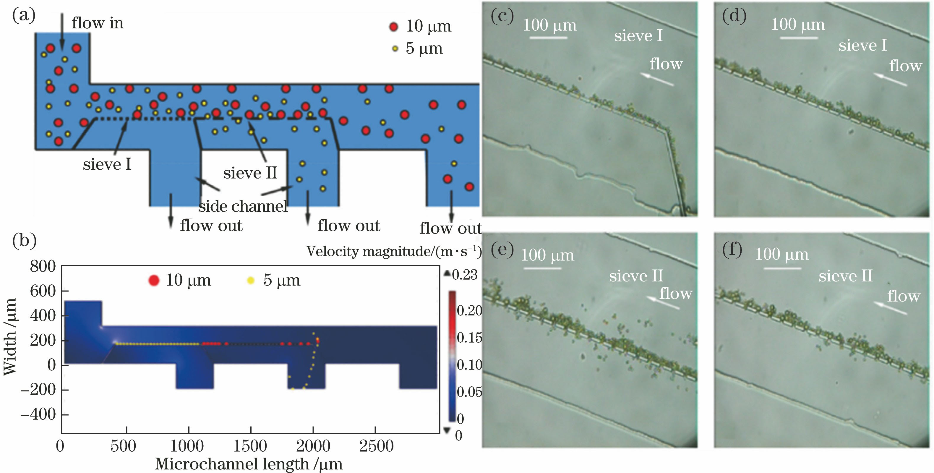
图 9. 超声微混合器。(a)混合装置照片;(b)混合装置剖面图;(c)具有设计结构的微通道剖面图;(d)荧光示踪剂显示的微柱周围流场
Fig. 9. Acoustic micromixer. (a) Photograph of mixing device; (b) cross-sectional schematic of mixing device; (c) cross-sectional schematic of microchannel with designed structure; (d) streaming-induced flow around micropillars visualized by fluorescent tracer particles
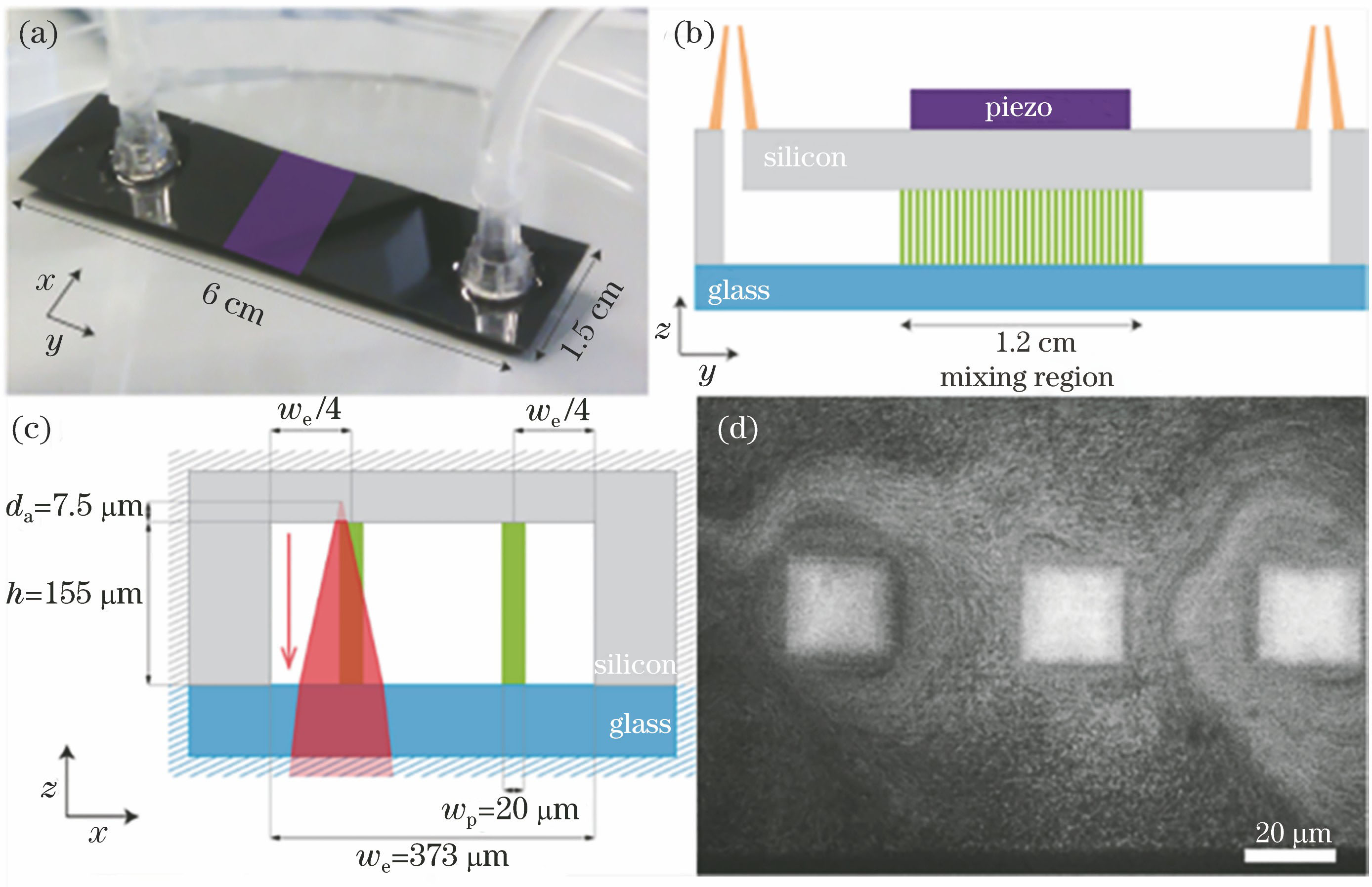
图 10. 新型微混合器。(a)新型3D混合元件的计算机辅助设计(CAD)图;(b)结构集成在管道中的SEM图像;(c)微混合器将去离子水(液体A)和罗丹明B染色的去离子水(液体B)混合后的光学显微镜图像
Fig. 10. Novel micromixer. (a) CAD rendering of novel 3D mixing element; (b) SEM image of structure integrated into microchannel; (c) optical image showing functionality of micromixer for de-ionized water (liquid A) and de-ionized water stained with Rhodamine B (liquid B)
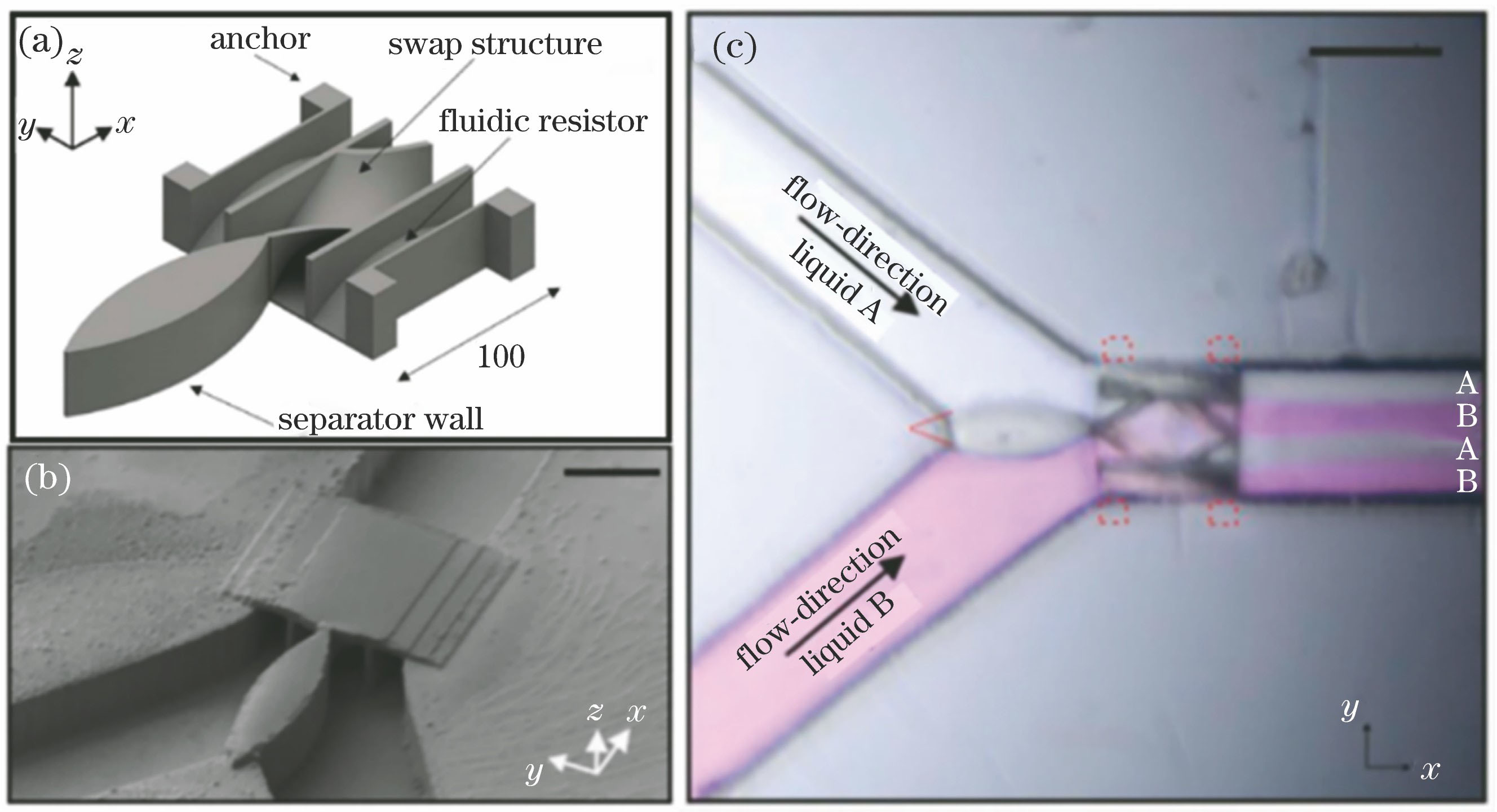
图 11. 微流量计。(a)微流量计的结构;(b)通道嵌入式流量计线路;(c)流量计随流速旋转的光学显微镜图像
Fig. 11. Schematics of microflowmeter. (a) Structure of microflowmeter; (b) flowmeter embedded in-line with microchannel; (c) optical images about rotation of flowmeter with different flow rates
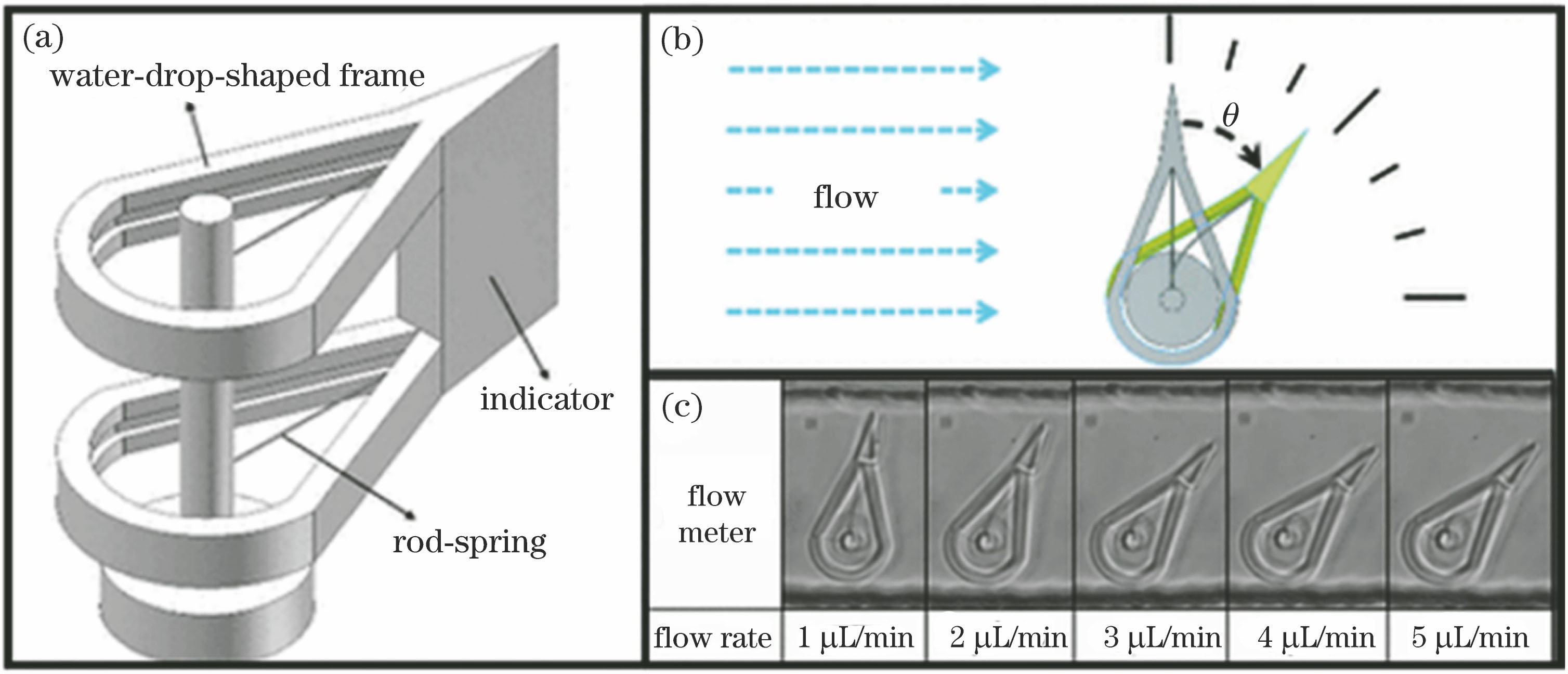
图 12. 弹簧状流量传感器。(a)飞秒激光双光子直写加工系统;(b) 3D弹簧状结构,直径为16 μm,节距为10 μm;(c)芯片实物图
Fig. 12. Spring-like flow sensor. (a) Femtosecond laser two-photon direct writing system; (b) 3D spring-like structure with diameter of 16 μm and pitch of 10 μm; (c) photo of chip
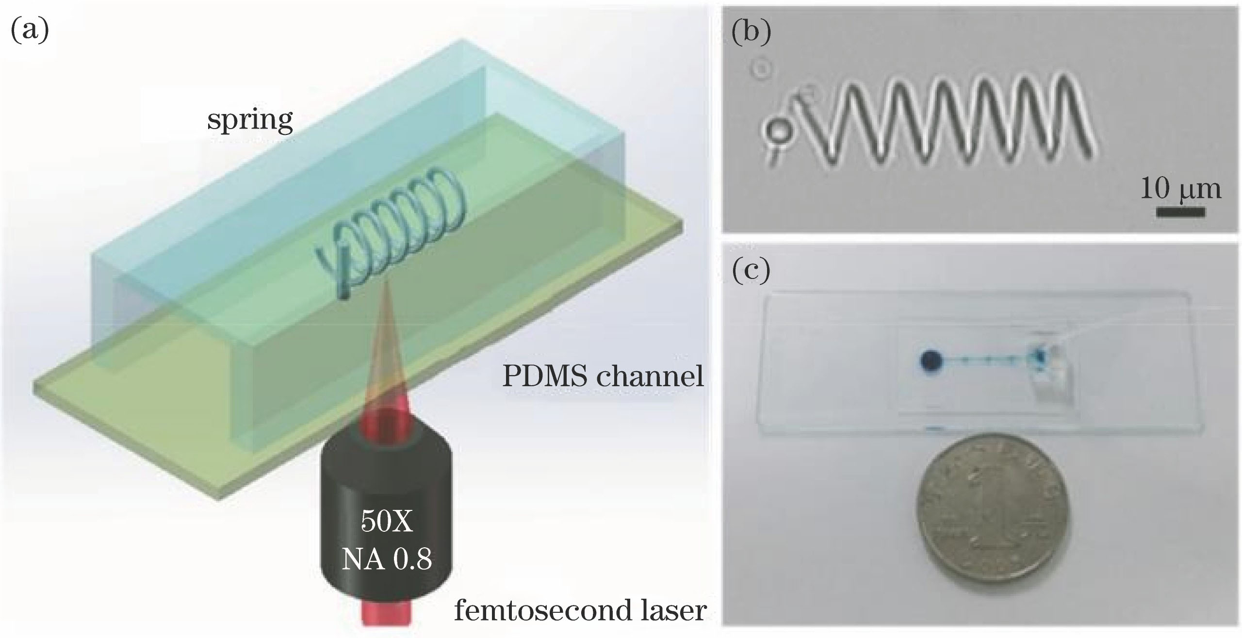
图 13. 微透镜及其功能。(a)PDMS微透镜在微流控设备中的集成;(b)焦距随不同溶剂溶解度的变化,插图为不同溶剂刺激后的PDMS微透镜的聚焦图像
Fig. 13. Microlens and its functionality. (a) Integration of PDMS microlens with microfluidic device; (b) dependence of focal length on solubilities of different solvents, in which insets are focused images of PDMS microlens after stimulation of different solvents
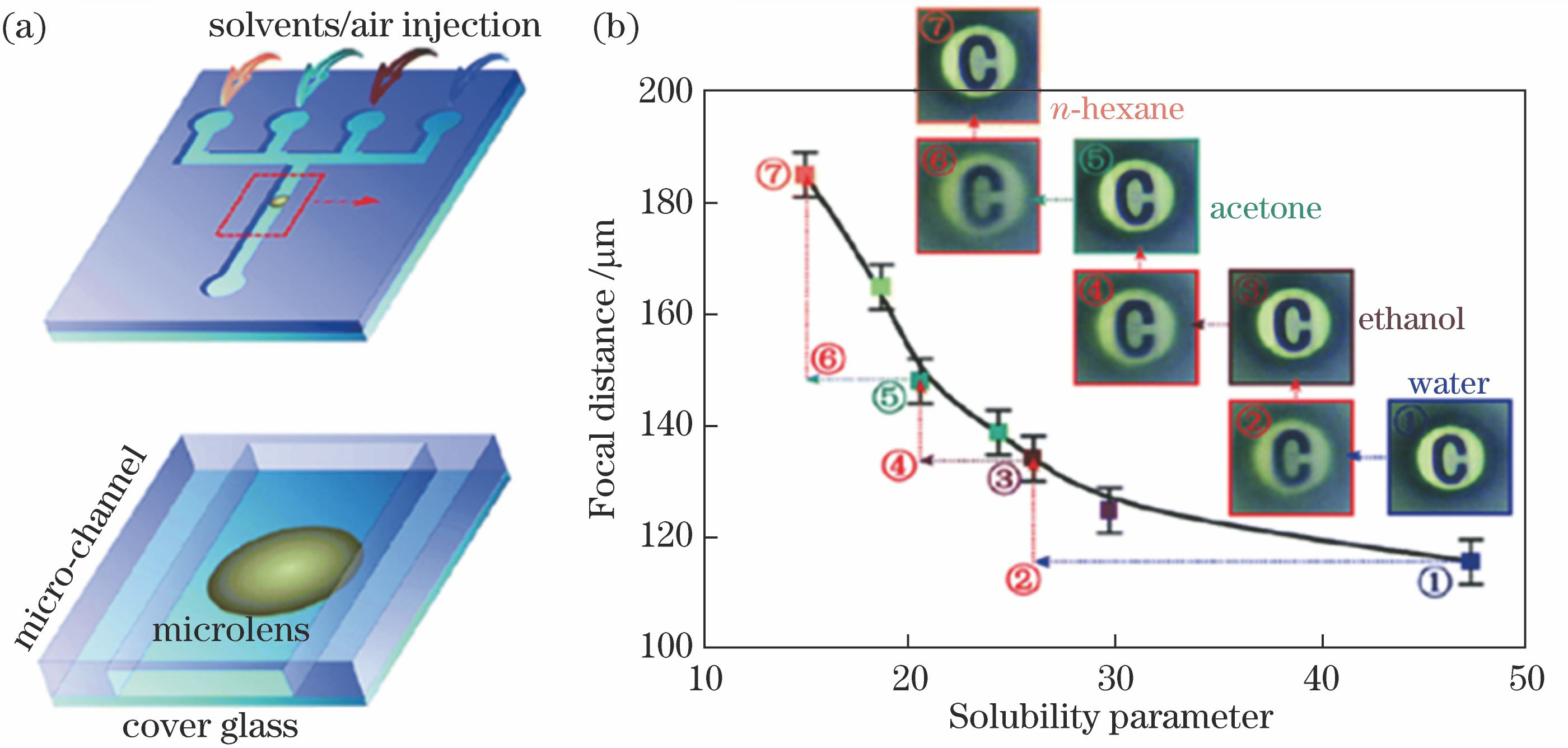
图 14. 中心通道结合微透镜阵列在玻璃微通道的集成。(a)结构设计;(b)密闭微管道的光学显微镜图像;(c)光流体在管道中的聚焦特性;(d)平面上局部结构的SEM图像;(e)光流体设备控制细胞位置的中通功能
Fig. 14. Integration of center-pass combined microlens array into glass microchannel. (a) Design of structure; (b) optical micrograph of closed microchannel; (c) focusing characteristic of optofluidic device in channel; (d) SEM image of local structure on flat surface; (e) center-pass function of optofluidic device to control cell position
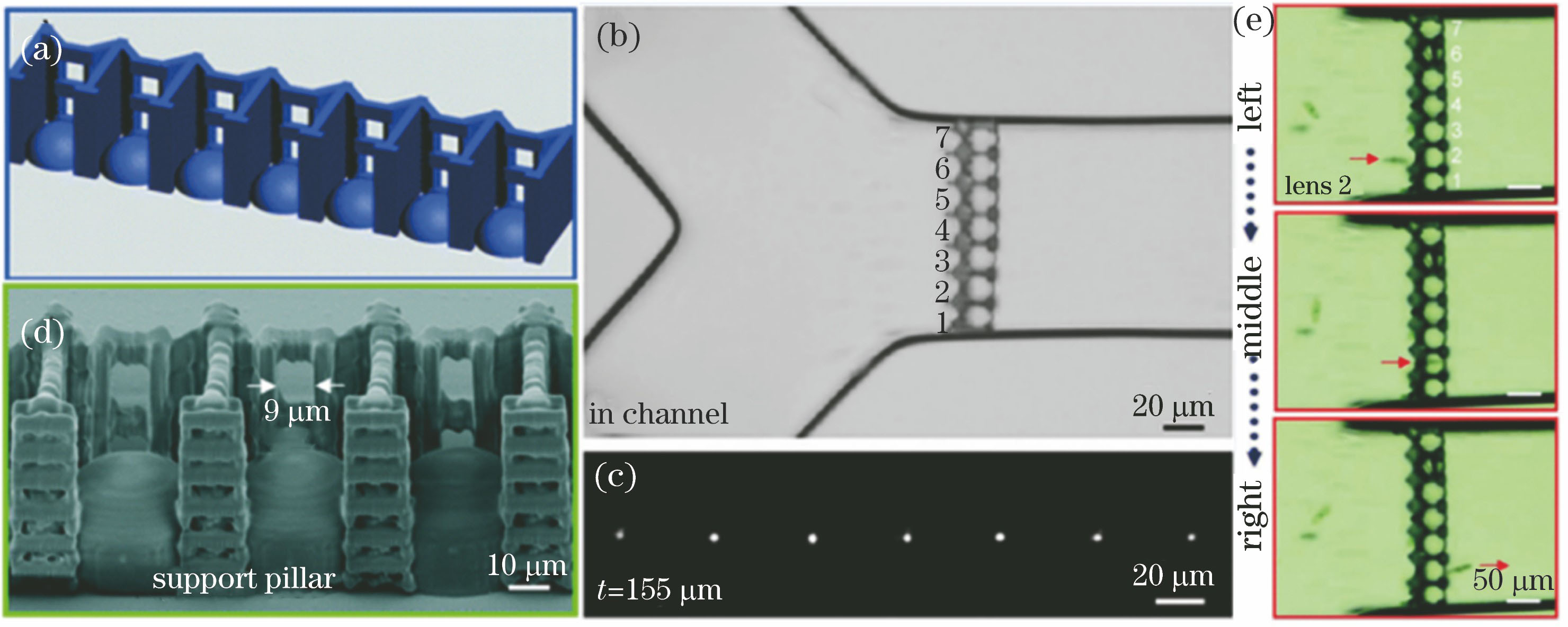
图 15. 微纤维芯片。(a)微流控管道中内嵌喷丝头的SEM图像;(b)直径为12 μm的喷嘴SEM图像特写;干燥处理后对折的纺丝纤维(c)SEM图像及(d)放大图;(e)未排列纤维和(f)排列纤维的光学显微镜图像
Fig. 15. Micro-fiber chip. (a) SEM image of spinneret embedded into microfluidic channel; (b) SEM image of close-up of nozzle tip with diameter of 12 μm; (c) SEM image of spun fiber that has broken in half after solvent drying and its (d) higher-magnification image; optical micrographs of (e) unaligned fiber and (f) aligned fibers
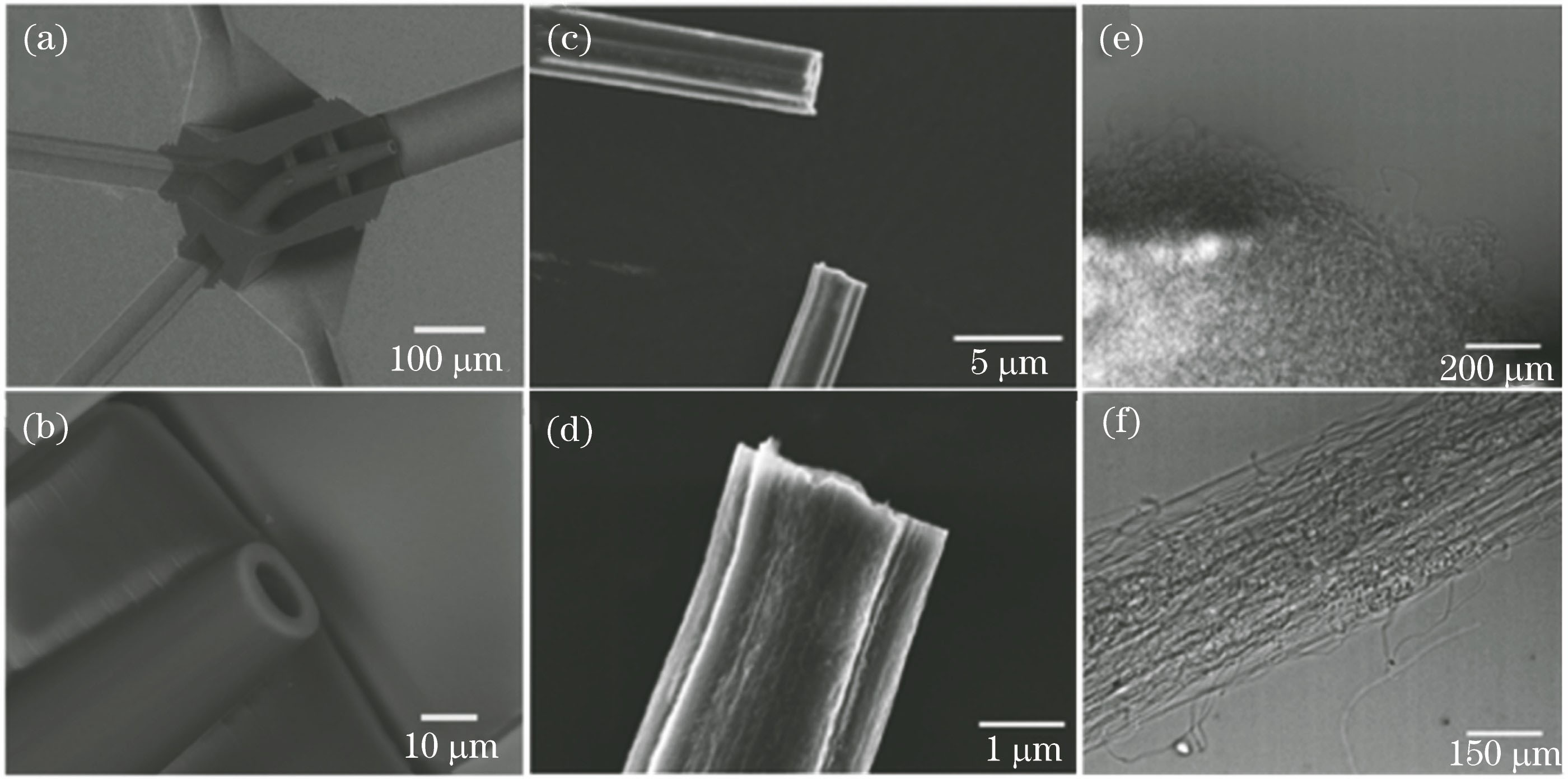
图 16. TPP的纳米壳结构。有洞半球的SEM图像(a)俯视图和(b)倾斜视图;(c)体积较大的长方体,制备时间仅为3 min;(d) 填充因子为100%的大面积六角微透镜阵列,制备时间仅为3 min
Fig. 16. Nano-shell structuring by TPP. (a) Top-view and (b) tilted-view SEM images of stand alone hemisphere with holes; (c) cuboid with large volume, whose fabrication time takes only 3 min; (d) hexagonal microlens array with fill-factor of 100% and large surface area, whose fabrication time takes only in 3 min
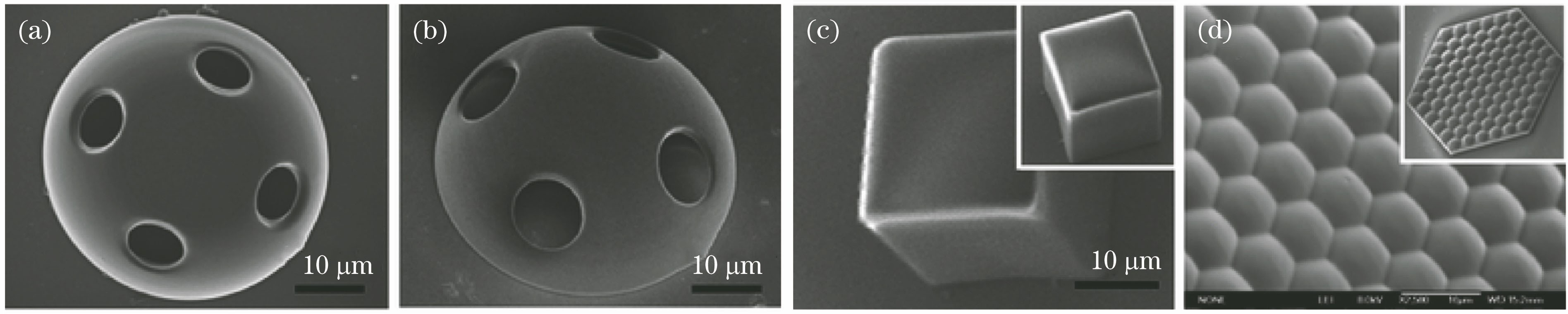
图 17. 多焦点并行加工示意图。(a)在SLM上显示一幅CGH图像,生成9个焦点,在给定的微通道内并行集成微观结构;(b) 9焦点并行加工的结构;(c) 5焦点加工微型过滤器;(d) 5焦点加工微型过滤器SEM图像;(e)直径为18.8 μm的癌细胞被微型过滤器阻拦的荧光显微镜图像
Fig. 17. Schematics of multi-foci parallel micro-fabrication. (a) Displaying CGH image on SLM, generating 9 foci to parallelly integrate microstructures inside given microchannel; (b) structures using 9-foci parallel fabrication; (c) microfilter using 5-foci parallel fabrication; (d) SEM image of microfilter using 5-foci parallel fabrication; (e) fluorescence microscope images of cancer cell with diameter of 18.8 μm blocked by microfilter
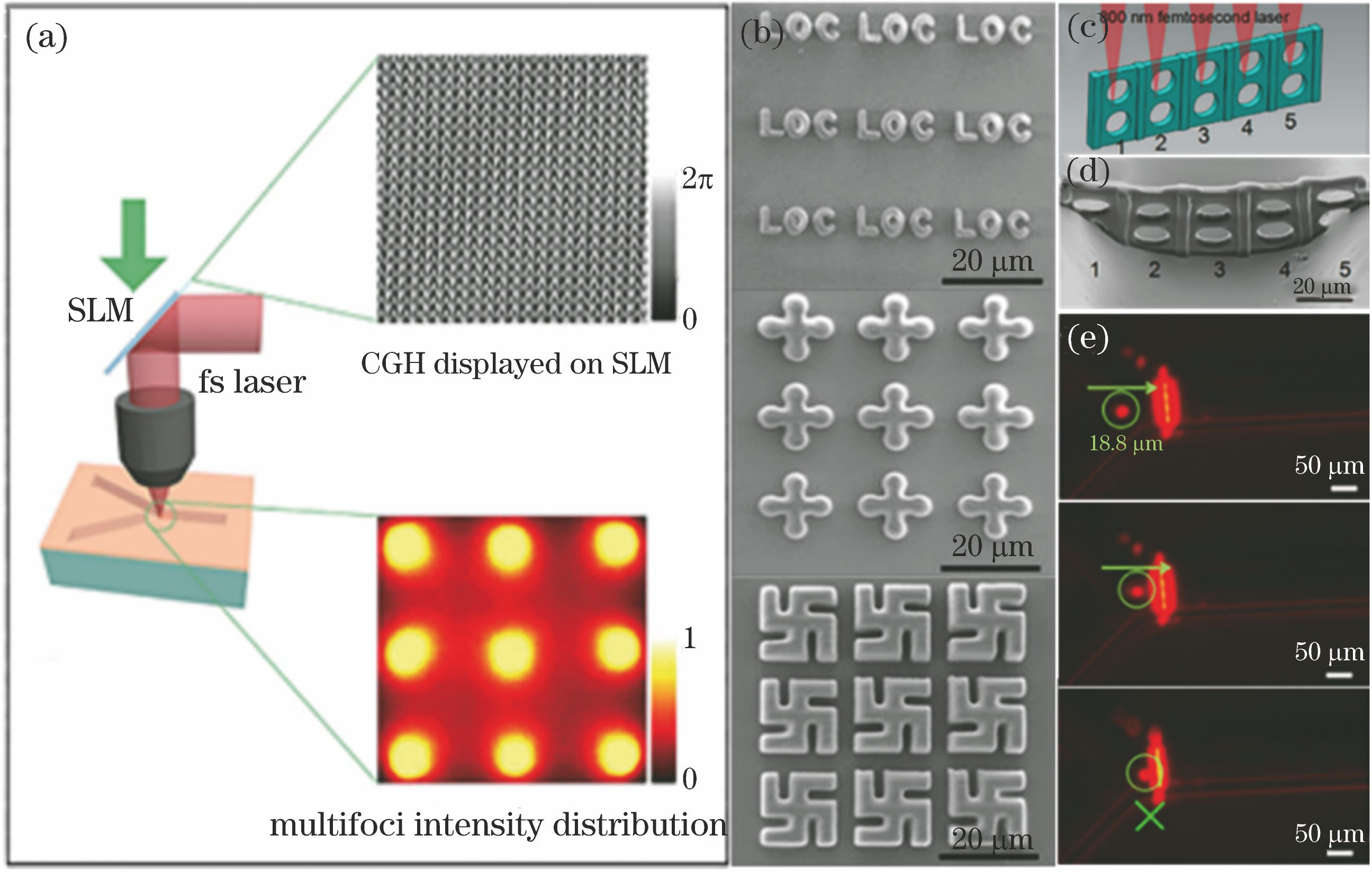
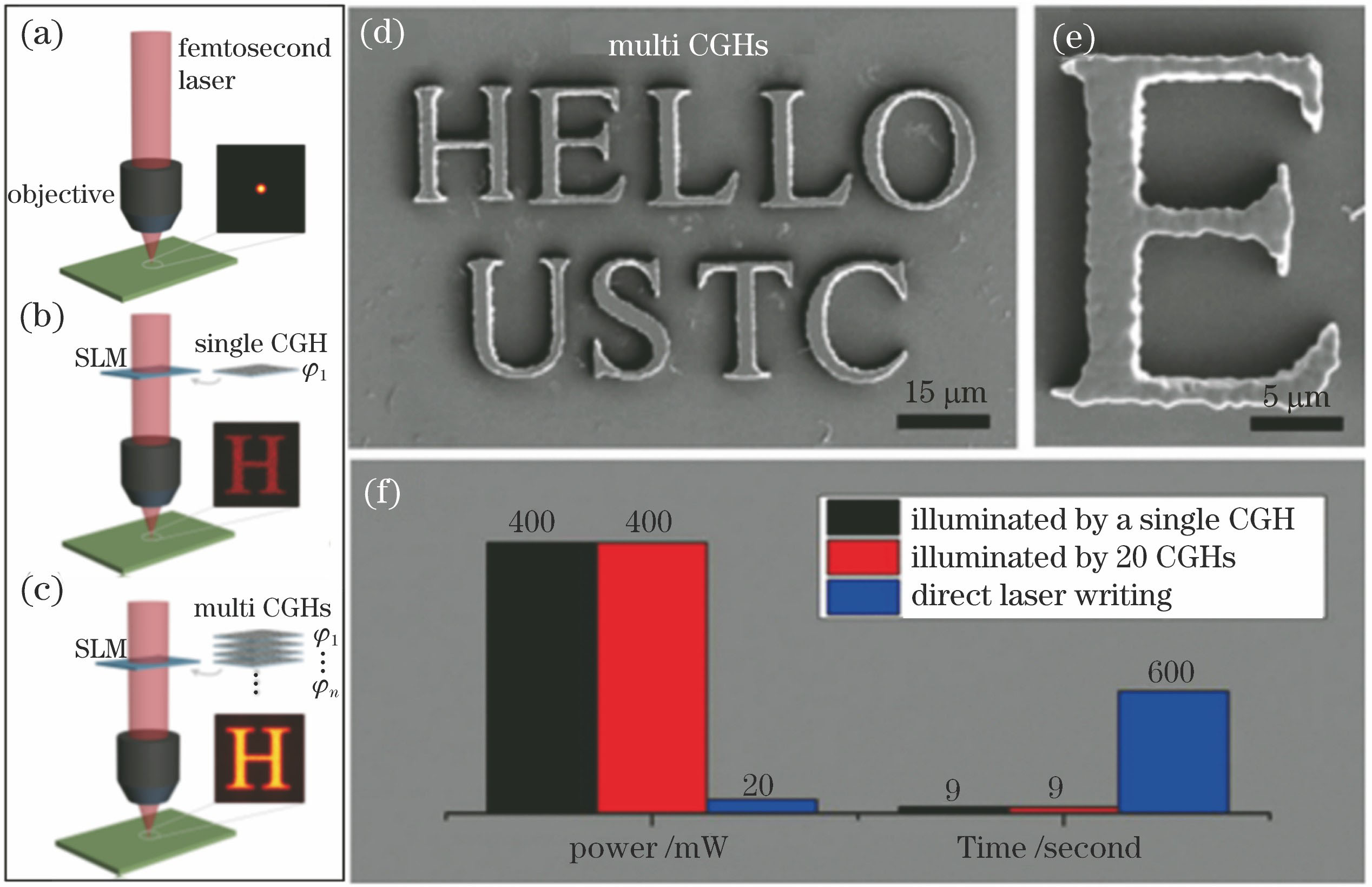
图 18. 3种加工方法示意图。(a)飞秒激光直写加工;(b)单次曝光全息飞秒激光直写图案;(c)多次曝光全息飞秒激光直写图案;(d)经多次曝光改善的SEM图像;(e)改善后字母E细节;(f) 3种加工方法的曝光能量、加工时间对比
Fig. 18. Schematics of three fabrication approaches. (a) Femtosecond laser direct writing; (b) single-exposure holographic femtosecond laser direct patterning; (c) multi-exposure holographic femtosecond laser direct patterning; (d) SEM image improved by multi-exposure; (e) detail of improved letter E; (f) comparison of corresponding laser power and fabrication time of three fabrication approaches
史杨, 许兵, 吴东, 肖轶, 胡衍雷, 姚成立. 飞秒激光直写技术制备功能化微流控芯片研究进展[J]. 中国激光, 2019, 46(10): 1000001. Yang Shi, Bing Xu, Dong Wu, Yi Xiao, Yanlei Hu, Chengli Yao. Research Progress on Fabrication of Functional Microfluidic Chips Using Femtosecond Laser Direct Writing Technology[J]. Chinese Journal of Lasers, 2019, 46(10): 1000001.


 PDF全文
PDF全文

