Mode division multiplexing: from photonic integration to optical fiber transmission [Invited]  Download: 880次
State Key Laboratory of Advanced Optical Communication Systems and Networks, Shanghai Jiao Tong University, Shanghai 200240, China
Figures & Tables
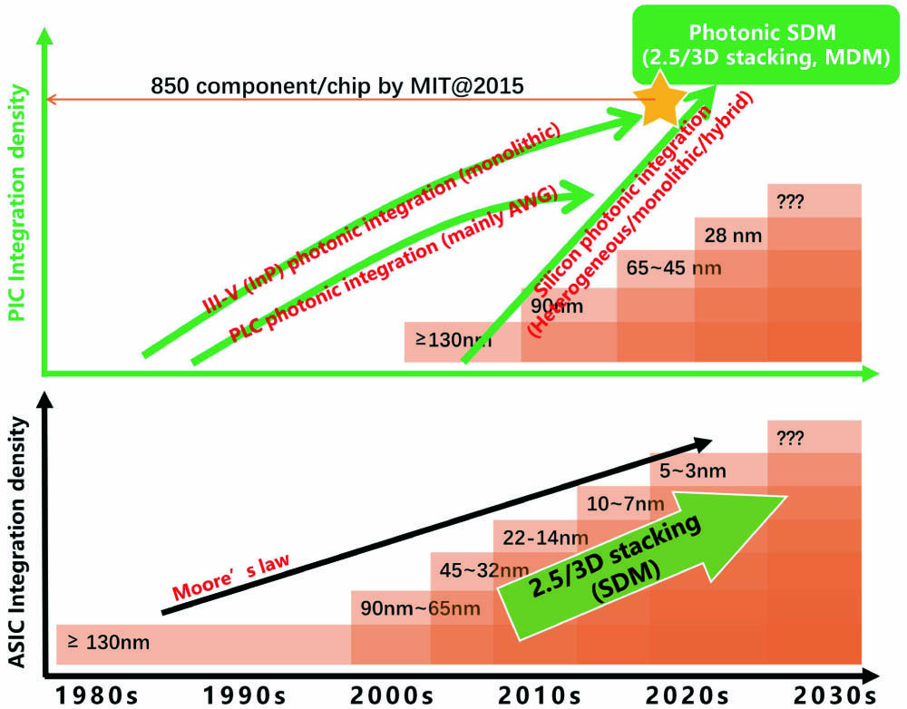
Fig. 1. Historical view of microelectronics development, PIC integration (upper), and ASIC integration (lower).
下载图片 查看原文
Fig. 2. Optical fiber transmission capacity trend with respect to all kinds of enabling technologies.
下载图片 查看原文
Fig. 3. Schematic diagram of MDM optical interface, including vertical coupling with on-chip mode multiplexer (MUX) and edge coupling with 3D asymmetric waveguide. (i)–(iii) Specific progresses of the MDM interface[35,36,37].
下载图片 查看原文
Fig. 4. Schematic diagram of integrated multimode waveguide bends: (a) the Euler curved bend for four TM modes[49], (b) the dual-mode bend with MC[54], (c) the pixelated four-mode bend structure[51], (d) four-mode bend based on a TIR mirror[56].
下载图片 查看原文
Fig. 5. Schematic diagram of integrated multimode waveguide crossing: (a) two-mode crossing based on non-adiabatic tapered waveguide[58], (b) three-mode crossing based on pixelated mode MUX and single-mode crossing array[60], (c) ultra-compact multimode crossing for two TE modes[61], (d) meta-material-based dual-mode star-crossing[62].
下载图片 查看原文
Fig. 6. Schematic diagram of integrated mode MUX/deMUX: (a) 10-channel mode (de)MUX with dual polarizations by adiabatic tapered ADC[15], (b) asymmetric Y-junction-based mode MUX[90], (c) MRRs serving as modulators and mode MUXs simultaneously[79], (d) four-mode MUX based on pixelated waveguides[86].
下载图片 查看原文
Fig. 7. Schematic diagram of universal (a) MC[94] and (b) mode exchanger[98].
下载图片 查看原文
Fig. 8. Schematic diagram of (a), (b) integrated PBS based on mode conversion[102,103] and (c) mode-transparent PBS based on TIR mirror[110].
下载图片 查看原文
Fig. 9. Schematic diagram of (a) Si-based MZI modulator with two branches of light propagating in one multimode waveguide[112], and (b) spatial mode recycling scheme used to reduce the required power consumption[113].
下载图片 查看原文
Fig. 10. Schematic of (a) mode switch based on two micro-rings[114] and (b) reconfigurable mode switch based on an MZI structure[115]. (c) Four-mode thermal switch by geometric-optic inspired multimode 3 dB coupler[56].
下载图片 查看原文
Fig. 11. Schematic diagram of Si optical phased array based on multi-pass recycling structure by mode multiplexing[119].
下载图片 查看原文
Fig. 12. Schematic diagram of integrated interconnect system hybrid multiplexed by WDM, MDM, and PDM.
下载图片 查看原文
Fig. 13. Schematic diagram of on-chip switching networks ROADM for multiplexing: (a) on-chip typical multimode optical switching system[125], (b) on-chip ROADM system for hybrid WDM and MDM[129].
下载图片 查看原文
Fig. 14. (a) Optimized step-index profiles of different FMFs[133], (b) core-cladding difference for seven-LP-mode fibers with step-index and depressed-inner-core profiles[134], (c) refractive index profile of ring-assisted four-mode fiber[135], (d) refractive index profile of ring-assisted seven-LP-mode fiber with trench structure[136].
下载图片 查看原文
Fig. 15. (a) Refractive index profile of two-mode graded-index fiber[137], (b) refractive index profile of nine-mode graded-index fiber with trench-assisted structure[138], (c) geometry and parameter definitions of the elliptical core fiber[142].
下载图片 查看原文
Fig. 16. Schematic of a multi-core super-mode fiber[143].
下载图片 查看原文
Fig. 17. (a) Flow chart of the proposed NN-assisted inverse design method. (b) The inverse design frame of the NN[145].
下载图片 查看原文
Fig. 18. Schematic diagram of mode MUX based on free-space beam combiner[148].
下载图片 查看原文
Fig. 19. Directional fiber-coupler-based (a) mode MUX and (b) mode deMUX supporting , a, and b modes[148].
下载图片 查看原文
Fig. 20. LPFBG-based (a) mode MUX and (b) mode deMUX supporting and a modes. MC is achieved by LPFBG[148].
下载图片 查看原文
Fig. 21. Schematic diagram of a photonics lantern[151].
下载图片 查看原文
Fig. 22. (a) Ring-shaped erbium doping profile[154]. (b) Refractive index and doping profile (shaded region) of the four-mode EDF[155]. (c) Overlaps between mode fields and gain media in a small doped area (left) and a large doped area (right)[156]. (d) Schematic of dual-core fiber with dual-core doping and colored shadings representing erbium doping[157]. (e) Schematic description of micro-structure[158].
下载图片 查看原文
Fig. 23. Schematic principle of DRA for mitigating the nonlinear distortion and noise over EDFA[148].
下载图片 查看原文
Fig. 24. Quasi-lossless transmission with bidirectional high-order pump[166].
下载图片 查看原文
Fig. 25. Inverse design based on NN for FM-DRA[170].
下载图片 查看原文
Fig. 26. Recent-year MDM experiments and progresses.
下载图片 查看原文
Table1. Photonic Integration Platforms
| | SOI | SiN | ChG | LN | InP |
|---|
| Index | 3.4 | 2.0 | 2–3 | 2.6 | 3.2 | | Loss (dB/cm) | 0.1 | | 0.05 | 0.027 | 0.3 | | Window (µm) | 1.1–3.7 | 0.4–2.4 | 1.5–12 | 0.4–5 | 1.3, 1.5 | | Lasing | No | No | No | No | Yes | | PD | Yes | No | No | No | Yes | | Modulation | Yes | No | No | Yes | Yes | | Extra doping | / | / | Standard process | Standard process | | CMOS compatibility | Yes | Yes | No | No | No |
|
查看原文
Table2. Cutting-Edge Performance of MDM Interface on SOI
| Properties | Vertical Coupling | Edge Coupling |
|---|
| Ref. [35] | Ref. [36] | Ref. [37] |
|---|
| Mode number | 6 | 4 | 2 | | Coupling loss | 20–25 dB | 4.9–6.1 dB | 10.77 dB | | Crosstalk | / | | −7.3 to −11.9 dB | | Bandwidth | | 20 nm | | | Footprint/length | mm-scale | | |
|
查看原文
Table3. Benchmark Performance of MDM Bend
| Properties | Euler Bend[49] | SWG Bend[50] | Pixelated Bend[51] |
|---|
| Structure and principle | Waveguide curve optimization | SWG for mode converting | Inverse design of pixelated structure | | Mode number | 4 TM modes | 6 modes with dual polarizations | 4 TE modes | | Bending radius | 45 µm | 10 µm | 3.9 µm | | Loss | | | | | Crosstalk | | | | | Scalability | Yes | Yes | Yes |
|
查看原文
Table4. The Summary of Mode MUX/deMUX
| Ref. | Year | L (μm) | (dB) | (dB) | BW (nm) | Channel | Structure | E / Sa |
|---|
| [9] | 2012 | 80 | 1 | | 50 | 2 (TE) | MMI + PS | S | | [68] | 2014 | 48.8 | 0.3 | | 100 | 2 (TE) | Symmetric Y junction + PS + MMI | S | | [69] | 2020 | 7.24 | 0.74–1.2 | | 50 | 2 (TE) | Shallow-etched MMI | E | | [70] | 2013 | 50 | 0.3 | | 100 | 2 (TE) | Adiabatic tapered ADC | E | | [72] | 2016 | 68 | 0.8–1.3 | | 65 | 2 (TE) | Taper-etched ADC | E | | [15] | 2018 | 15–50 | 0.2–1.8 | −15 to −25 | 90 | 10 (PM) | Adiabatic tapered ADC | E | | [71] | 2019 | 75 | 1.5 | / | 75 | 12 (TE) | Adiabatic ADC using SWG | E | | [73] | 2013 | | 1.5 | | 100 | 2 (TE) | Asymmetric Y junction | E | | [74] | 2016 | 510 | 5.7 | −9.7 to −31.5 | 29 | 3 (TE) | Cascaded asymmetric Y junction | E | | [12] | 2013 | 300 | 0.3 | | 100 | 2 (TE) | Adiabatic coupler | E | | [75] | 2016 | 200 | 1 | | 75 | 2 (TE) | Adiabatic coupler + Y junction | E | | [76] | 2017 | 180 | 1.5 | | 90 | 2 (TE) | Adiabatic coupler + Y junction | E | | [77] | 2014 | 25 | 3–16 | −12 to −22 | / | 3 (TE) | Micro-ring | E | | [78] | 2015 | 100 | 1.5–3.5 | −20 to −32 | / | 3 (TE) | Micro-ring | E | | [79] | 2019 | 40 | 2.1 | | / | 4 (TE) | Micro-ring | E | | [81] | 2013 | 90–250 | 0.2–0.34 | −22 to −30 | 3.7–11.8 | 4 (TE) | Grating-assisted contra-DC | S | | [82] | 2015 | / | / | | / | 2 (TE) | Grating-assisted tapered contra-DC | E | | [83] | 2020 | 300 | 6.6 | | | 4 (PM) | SWG-based contra-DC | E | | [84] | 2016 | | 1.2 | | 100 | 2 (TE) | Topology optimized structure | E | | [85] | 2018 | | 1.2–2.5 | | 60 | 3 (TE) | Pixelated structure | E | | [86] | 2020 | | 1.5 | | 60 | 4 (TE) | Pixelated structure | E | | [87] | 2018 | | 4 | | 40 | 2 (TE) | Triple waveguide coupler | E | | [88] | 2018 | 7.5 | 0.32 | | 35 | 2 (TM) | Triple waveguide coupler with hybrid plasmonic waveguide | S |
|
查看原文
Jiangbing Du, Weihong Shen, Jiacheng Liu, Yufeng Chen, Xinyi Chen, Zuyuan He. Mode division multiplexing: from photonic integration to optical fiber transmission [Invited][J]. Chinese Optics Letters, 2021, 19(9): 091301.


 PDF全文
PDF全文

