Silicon photonic platforms for mid-infrared applications [Invited]  Download: 1118次
1 Institute of Microelectronics, Agency for Science, Technology and Research (A*STAR), 2 Fusionopolis Way, #08-02, Innovis, Singapore 138634, Singapore
2 Department of Electrical & Computer Engineering, National University of Singapore, 4 Engineering Drive 3, Singapore 117583, Singapore
Figures & Tables
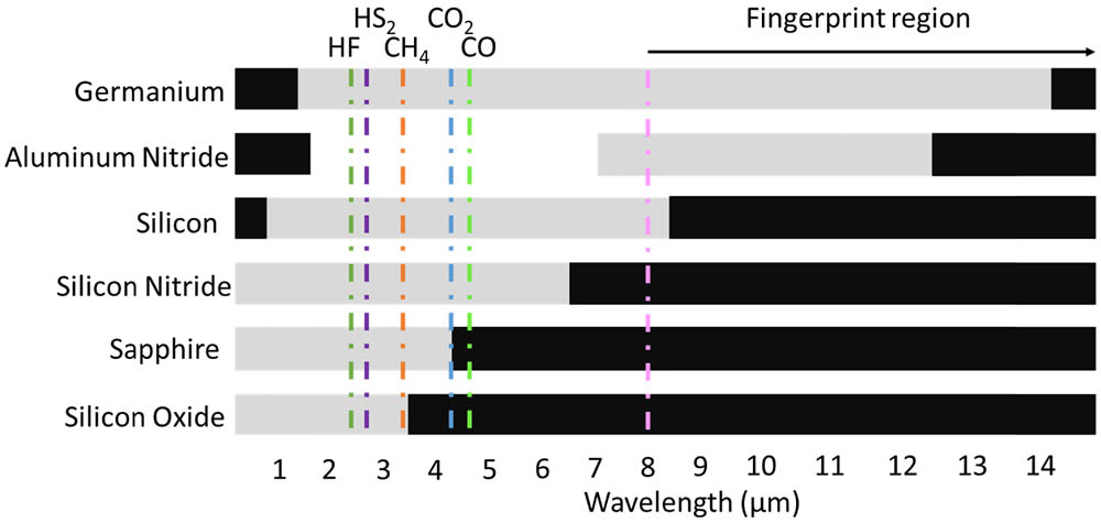
Fig. 1. Material absorption characteristic in the MIR range [1,3]. Gray region represents the optical transparency; black area denotes the high loss. Absorption peaks of some detected gases and the fingerprint region are marked.
下载图片 查看原文
Fig. 2. (a) Fabricated 8-in. silicon wafer with MIR devices after wafer dicing for characterization. (b) SOI strip ring resonators and rib DCs. (c) SOI strip DCs, bends, waveguides, and rib waveguides. (d)–(k) SEM images of the fabricated devices. (d) SOI waveguide taper tip. (e) SOI strip waveguide. (f) SOI rib waveguide. (g) SOI rib DC. (h) SOI strip to rib converter. (i) SOI strip DC array. (j) SNOI DC. (k) SNOI add–drop ring resonator.
下载图片 查看原文
Fig. 3. Loss characterization of SOI waveguide. (a) Propagation loss of SOI strip waveguide. (b) Bending loss of SOI strip waveguide. (c) Propagation loss of SOI rib waveguide. Insets in (a) and (c) show the corresponding mode field simulated by the commercial software Lumerical FDTD.
下载图片 查看原文
Fig. 4. Characterization of SOI strip and rib DCs. (a) and (c) Self-normalized transmitted and coupled power of (a) strip and (c) rib DCs. Solid lines show sine squared fitting of the data with adjusted R-square of 0.997. (b) and (d) Power coupling coefficient K of (b) strip and (d) rib DCs. Insets show the linear fitting of Y with respect to Lc with the extracted parameters Lπ and Ø0.
下载图片 查看原文
Fig. 5. Characterization of SOI strip racetrack resonators. Red dots present measurement data, while the blue solid lines show fitting results. (a) and (c) Transmission spectra of the racetrack resonator with (a) r=5 μm, g=500 nm, and Lc=50 μm, (c) r=5 μm, g=550 nm, and Lc=10 μm. (b) and (d) Zoom-in of a particular resonating wavelength at ∼3687 nm in (a) and ∼3824 nm in (c) as indicated by the navy blue square box.
下载图片 查看原文
Fig. 6. Loss characterization of SNOI waveguide. (a) Propagation loss of SNOI strip waveguide. (b) Bending loss of SNOI strip waveguide. Inset in (a) shows the mode field simulated by Lumerical.
下载图片 查看原文
Fig. 7. Characterization of the SNOI strip ring resonator with radius of 20 μm and coupling gap of 550 nm. Transmission spectrum of the ring resonator (a) from 1960 to 2045 nm with scanning step of 0.54 nm (b) around the resonance of 1988 nm with scanning step of 0.011 nm.
下载图片 查看原文
Fig. 8. CO2 gas sensors based on MIR photonics. Sensor configuration with the (a) spiral waveguide and (c) MRR. (b) Detected optical power variation versus CO2 concentration of the sensor shown in (a). (d) Q-factor variation and effective gas interaction length varying with CO2 concentration of the sensor shown in (b).
下载图片 查看原文
Table1. Demonstrated MIR Waveguides with Various Platforms
| No. | Platform | Structure Type | Cross-Section Size (μm×μm) | Working Wavelength (μm) | Loss (dB/cm) | Pol. | Year | Ref. | | 1 | SOI | Strip | | 2.1 | 0.6 | TE | 2012 | [5] | | 2 | SOI | Rib | () | 2 | 1 | TE | 2016 | [6] | | 3 | SOI | Rib | () | 3.39 | 0.6–0.7 | TE/TM | 2011 | [7] | | 4 | SOI | Rib | () | 3.73 | | TE | 2012 | [8] | | 5 | Rib | () | 3.8 | | | 6 | Strip | | 3.74 | | | 7 | SOI | Suspended Rib | () | 2.75 | | TE | 2012 | [9] | | 8 | SOI | Rib | () | 3.76 | 5.3 | TE | 2013 | [10] | | 9 | Strip | | 3.1 | | 10 | SOI | Slot | , ( μm) | 3.8 | | Slot Mode | 2015 | [11] | | 11 | SOI | Strip | | 3-4 | | TE | 2017 | [12] | | 12 | SOI | Strip | | 3.75 | | TE | 2017 | [13] | | 13 | Rib | () | | | 14 | GOS | Strip | | 5.8 | 2.5 | TM | 2012 | [32] | | 15 | GOS | Rib | , () | 3.8 | 0.6 | TE | 2015 | [33] | | 16 | GOI | Strip | | 3.682 | | TE/TM | 2016 | [34] | | 17 | GOI | Strip | | 3.682 | | TE/TM | 2016 | [35] | | 18 | GOI | Rib | () | 2 | 14 | TE | 2016 | [36] | | 19 | GOSN | Strip | | 3.8 | | TE | 2016 | [37] | | 20 | SOSN | Rib | () | 3.39 | | TE/TM | 2013 | [38] | | 21 | SOS | Strip | | 4.5 | | TE | 2010 | [39] | | 22 | SOS | Strip | | 5.18 | 1.92 | TE | 2011 | [40] | | 23 | SGOS | Strip | | 4.5 | 1 | TM | 2014 | [41] | | 24 | | 7.4 | 2 |
|
查看原文
Table2. Demonstrated MIR MRRs with Various Platforms
| No. | Platform | Bending Radius (μm) | Working Wavelength (μm) | Maximum -Factors (a.u.) | ER (dB) | FSR (nm) | Pol. | Year | Ref. | | 1 | SOI | 100 | 3.74 | 8200 | 4–9 | 4.12 | TE | 2012 | [8] | | 2 | SOI | 40 | 2.75 | 8100 | NA | NA | TE | 2012 | [9] | | 3 | SOI | NA | 3.5–3.8 | | | NA | TE | 2017 | [12] | | 4 | SOI | | 5.2 | 2700 | NA | NA | TE | 2013 | [14] | | 5 | 3.4 | 7900 | | 6 | SOI | 20, 30, 40 | 3.7–3.8 | 2900 | | 5.33 | TE | 2014 | [17] | | 7 | GOS | 52, 142, 149 | | 1672 | 17.46 | 7.7 | TE | 2016 | [18] | | 8 | SOS | 40 | 5.4–5.6 | 3000 | NA | 29.7 | TE | 2010 | [51] | | 9 | SOS | 150 | 2.75 | | NA | NA | TE | 2012 | [52] | | 10 | SOS | 60 | 4.4–4.6 | | NA | 12.4 | NA | 2013 | [53] |
|
查看原文
Ting Hu, Bowei Dong, Xianshu Luo, Tsung-Yang Liow, Junfeng Song, Chengkuo Lee, Guo-Qiang Lo. Silicon photonic platforms for mid-infrared applications [Invited][J]. Photonics Research, 2017, 5(5): 05000417.


 PDF全文
PDF全文

