Chinese Optics Letters, 2021, 19 (2): 021301, Published Online: Jan. 4, 2021  

Multi-gigahertz laser generation based on monolithic ridge waveguide and embedded copper nanoparticles Download: 701次

Author Affiliations
1 School of Physics, State Key Laboratory of Crystal Materials, Shandong University, Jinan 250100, China
2 Collaborative Innovation Center of Light Manipulations and Applications, Shandong Normal University, Jinan 250358, China
3 Key Laboratory of Materials for High-Power Laser, Shanghai Institute of Optics and Fine Mechanics, Chinese Academy of Sciences, Shanghai 201800, China
4 Department of Physics, Center for Ion Beam Application and Center for Electron Microscopy, Wuhan University, Wuhan 430072, China
Abstract
Copper (Cu) nanoparticles (NPs) are synthesized under the near-surface region of the Nd:Y3Al5O12 (Nd:YAG) crystal by direct Cu+ ions implantation. Subsequently, the monolithic ridge waveguide with embedded Cu NPs is fabricated by C4+ ions irradiation and diamond saw dicing. The nonlinear optical response of the sample is investigated by the Z-scan technique, and pronounced saturable absorption is observed at the 1030 nm femtosecond laser. Based on the obvious saturable absorption of Cu NPs embedded Nd:YAG crystal, 1 μm monolithic mode-locked pulsed waveguide laser is implemented by evanescent field interaction between NPs and waveguide modes, reaching the pulse duration of 24.8 ps and repetition rate of 7.8 GHz. The work combines waveguides with NPs, achieving pulsed laser devices based on monolithic waveguide chips.

1. Introduction

In the past few years, dielectric waveguide lasers have been well investigated by researchers to realize diverse applications in a number of areas[14" target="_self" style="display: inline;">4]. As the compact and integratable laser source, the waveguide laser has superior laser performances compared with the bulk laser, such as lower lasing threshold and higher slope efficiency[59" target="_self" style="display: inline;">9]. In addition, the mode of the waveguide laser can be tailored in a flexible manner according to the practical requirements[10,11]. Various saturable absorbers (SAs) and laser gain media have been utilized in waveguide systems for passively Q-switched and mode-locked laser generation. A wide range of the spectral region has been obtained from visible to mid-infrared for integrated optoelectronic devices[1214" target="_self" style="display: inline;">–14]. According to the dimensionality, SAs can be classified into zero-dimensional (0D) materials [e.g.,  quantum dots and nanoparticles (NPs)], one-dimensional (1D) materials [e.g.,  carbon (C) nanotubes], two-dimensional (2D) materials (e.g.,  graphene and black phosphorus), and three-dimensional (3D) materials[1523" target="_self" style="display: inline;">23]. Particularly, metallic NPs possess unique and distinct optical properties such as saturable absorption and the localized surface plasmon resonance (LSPR) effect, which enable them to be promising candidates in ultrafast photonic applications[2429" target="_self" style="display: inline;">29]. Plasmonic NPs can be fabricated by a variety of techniques, including vacuum electron-beam co-evaporation method, melt-quenching technique, nanosphere lithography, colloidal chemical synthesis, ion implantation, etc.[30,31]. Among them, ion implantation, as one of the most efficient ways, shows unique advantages such as perfect air stability, controllability of fluence and energy, and selectivity of the substrate[32,33]. NPs can be synthesized directly by ion implantation or subsequent annealing treatment. The physical properties of the substrate can also be modified by ion implantation. For example, the nonlinearity of the substrate can be modulated by embedded NPs, owing to the LSPR effect. Recently, copper (Cu) NPs were synthesized in lithium tantalate crystal by direct ion implantation, and the nonlinear optical response can be modulated by increasing implanted ion fluence and swift heavy ion irradiation. Based on the nonlinear absorption properties of NPs and waveguide configuration, Q-switched waveguide lasers have been widely reported over a variety of gain media[34]. Monolithic waveguide laser devices are required to achieve on-chip lasing. Recently, silver (Ag) NPs were embedded in the Nd:Y3Al5O12 (Nd:YAG) crystal together with subsequent O5+ ions irradiation and diamond blade dicing for the fabrication of ridge waveguiding structures, achieving pulsed laser generation based on a monolithic waveguide chip[35]. With the unique advantage of being cost effective and economical, Cu NPs own superior LSPR absorption peaks at longer wavelengths compared with gold (Au) and Ag NPs. It means that the Cu NPs may have stronger linear and nonlinear optical response at the near-infrared band[36]. These advantages of Cu NPs attract the interest of researchers as efficient SAs for the modulation of nonlinear optical response and generation of the monolithic mode-locked waveguide laser. In this work, Cu+ ions were implanted into the Nd:YAG crystal by normal incidence and synthesized Cu NPs. The subsequent processing of the C4+ ions irradiation and diamond saw dicing lead to the fabrication of monolithic waveguides in the Nd:YAG crystal with embedded Cu NPs. Finally, the monolithic waveguide laser at 1 µm was implemented based on the evanescent field interaction between Cu NPs and the waveguide mode.

2. Experiment

The Nd:YAG crystal was used in this work, which was cut with dimensions of 10mm×10mm×2mm [Fig. 1(a)]. The sample was implanted with Cu+ ions with energy of 100 keV and fluence of 1×10¹⁷ions/cm2 [Fig. 1(b)]. During the ion implantation process, when the implantation dose is high and the concentration is above the solubility limit, the implanted impurity atoms will aggregate to form NPs. After that, C ions (C4+) with fluence of 6×10¹⁴ions/cm2 and energy of 15 MeV are irradiated into the sample, forming the planar optical waveguide with a thickness of 10μm beneath the Nd:YAG crystal surface, as shown in Fig. 1(c). Finally, a rotating diamond blade with high speed (2000 r/min) was employed to fabricate the ridge optical waveguide with a width of 23.5 µm by manufacturing parallel air grooves on the planar waveguide surface. The corresponding schematic diagram is depicted in Fig. 1(d).
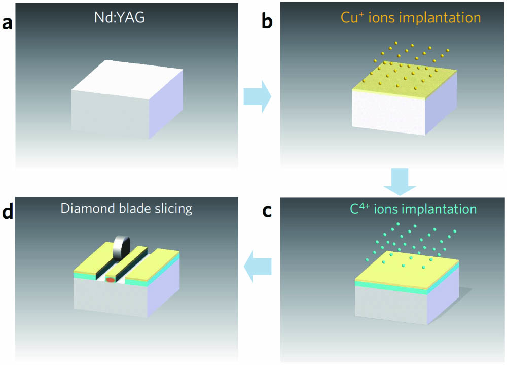
Fig. 1. Schematic of the sample fabrication. (a) Pure Nd:YAG. (b) Cu+ ions implantation. (c) C4+ ions irradiation. (d) Diamond blade slicing.

下载图片 查看所有图片

Figure 2(a) shows the transmission electron microscopy (TEM) image of Cu NPs embedded YAG crystal. As indicated, the synthesized Cu NPs are mainly distributed at the depth between 50 nm and 125 nm under the surface of the sample. The element mapping image of the sample is shown in Fig. 2(b), which further confirms the formation of Cu NPs in the YAG crystal. Figure 2(c) depicts the high-resolution TEM (HRTEM) image. The interplanar spacing (d) of a single NP is calculated to be 0.21 nm, as depicted in the inset, which is well consistent with the crystal orientation (200) of Cu from a standard data card (PDF#040836). The diameter distribution of synthesized Cu NPs is displayed in Fig. 2(d), and the main diameter is 2.16 nm.
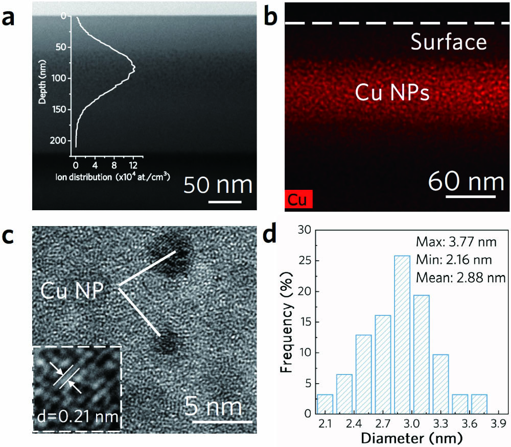
Fig. 2. (a) TEM image of the sample and projection distribution of implanted Cu+ ions. (b) Cu element distribution mapping. (c) HRTEM image. (d) Diameter distribution of NPs.

下载图片 查看所有图片

3. Results and Discussion

The linear optical absorption of the Cu NPs embedded in the Nd:YAG waveguide is measured and simulated simultaneously. As indicated in Fig. 3(a), the LSPR absorption of Cu NPs shows a broad band with the peak position located at 592 nm. The inset shows the picture of the sample. It can be seen that there are a few parallel air grooves on the sample surface, which are constructed by diamond blade slicing for ridge waveguide fabrication. The absorption spectrum can be simulated by the Mie theory: where p represents the volume fraction of metal (p=0.1). λ0 is the wavelength of light in vacuum. ϵd and ϵm denote the complex dielectric constants of insulator and metal, respectively[37]. The simulation result is depicted in Fig. 3(b). The simulated LSPR peak of Cu NPs embedded in Nd:YAG is at 590 nm, which is consistent with the experimental result.
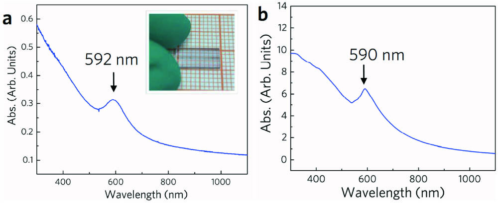
Fig. 3. (a) Measured linear optical absorption spectrum. Insert is the picture of the sample. (b) Calculated linear optical absorption spectrum.

下载图片 查看所有图片

The open-aperture (OA) Z-scan system operated at 1030 nm is used to measure the ultrafast nonlinear optical absorption of samples, and the corresponding schematic diagram is depicted in Fig. 4(a). The experiment was carried out using a mode-locked femtosecond laser with the repetition rate of 1 kHz and pulse width of 340 fs. The beam waist radius at the focus is measured to be 30μm. As shown in Fig. 4(b), there is no obvious nonlinear optical response for the sample without Cu+ ions implantation at 1030 nm. However, saturable absorption is revealed for the sample with Cu NPs (Cu-C-Nd:YAG), which indicates significant potential in photonic devices. The saturation intensity (Is) can be obtained by fitting the nonlinear optical response curve by the equation[38]where α0 is the linear absorption coefficient, and I is the laser intensity at different positions (z). The saturation intensity is calculated to be 12.9GW/cm2 at energy of 50 nJ, and the modulation depth is 1.5%.

Fig. 4. (a) Schematic of OA Z-scan system. (b) The nonlinear optical response of samples under the excitation of 340 fs pulses at 1030 nm.

下载图片 查看所有图片

Based on the saturable absorption of Cu NPs, the implanted layer can be regarded as SAs and integrated on the dielectric optical waveguide. Utilizing the evanescent field coupling effect, mode-locking operation can be implemented in a tiny volume without an additional modulator. As shown in Fig. 5(a), an 808 nm continuous wave (CW) laser is coupled into the waveguide for the excitation of photons at 1064 nm. With the oscillation of photons in the laser cavity, the CW laser at 1064 nm is generated and propagated along the x axis according to the total internal reflection. During the process, some photons will tunnel the potential barrier and propagate along interface between the NP layer and waveguide layer with certain distance (i.e., Goos–Hanchen shift)[39], resulting in the formation of evanescent waves. Therefore, the Cu NPs can interact with the evanescent wave sufficiently and realize the modulation of a 1064 nm CW laser for mode-locked layer generation. The evanescent field coupling effect can be demonstrated by the near-field distribution simulated by the COMSOL Multiphysics® software, as depicted in Figs. 5(b) and 5(c). It is obvious that the near-field intensity is decreased by one-order magnitude after implantation of Cu NPs. The evanescent wave is absorbed by the NPs due to the LSPR induced saturable absorption, which indicates the potential for integration of NPs and dielectric waveguide.
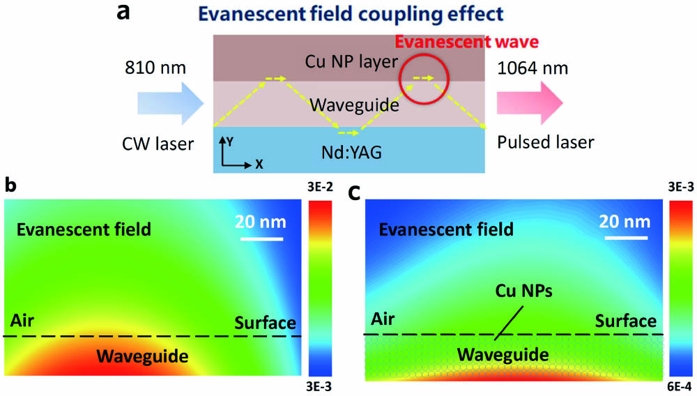
Fig. 5. (a) Schematic of evanescent field coupling effect. (b) Near-field distribution of the sample without Cu NPs. (c) Near-field distribution of the sample with Cu NPs.

下载图片 查看所有图片

The end-face coupling system was used to implement the 1 µm mode-locked pulsed laser generation with the pump laser at 808 nm. The laser cavity was formed by input mirror M1 (transmission of 98% at 808 nm and reflectivity of 99% at 1064 nm) and output mirror M2 (transmission of 90% at 1064 nm). The generated pulsed laser was collected and displayed by a digital oscilloscope. Figure 6(a) depicts the output power of the generated mode-locked pulsed laser as a function of the launched power. As shown, the laser threshold is 214 mW. As the launched power increases linearly to 836 mW, the output power is up to 58 mW. The emission spectrum of the output waveguide laser is displayed in Fig. 6(b), which centers at 1064 nm and corresponds to the main emission line of the Nd3+ ion F43/2I411/2 transition. The measured near-field modal profile of the ridge waveguide is shown in the inset. Figure 6(c) indicates the single Q-switched envelope on the nanosecond (20 ns/div) time scale under the launched power of 450 mW. Figure 6(d) shows the measured mode-locked pulse train on the time scale of 400 ps/div, and the pulse duration of a single pulse is as short as 24.8 ps. The fundamental repetition rate is 7.8 GHz, and the signal-to-noise ratio is up to 47.8 dB, indicating excellent mode-locking stability. The waveguide loss was calculated by the following equation: where Pin and Pout represent in-coupled power and output power, respectively. The waveguide loss at the TM polarization is as low as 0.68 dB, which suggests superior waveguide properties at 1064 nm.
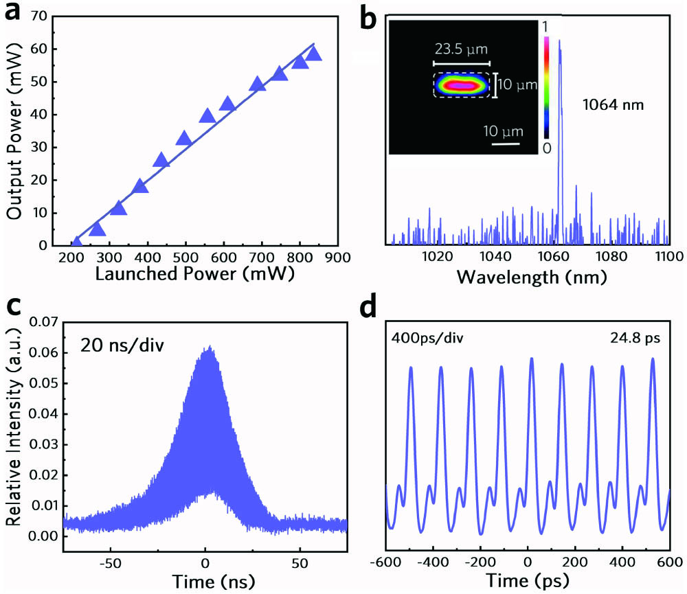
Fig. 6. (a) Output power as a function of the launched power. (b) The emission spectrum of the output waveguide laser. Inset is the near-field modal profile. (c) Single Q-switched envelope on the nanosecond time scale under the launched power of 450 mW. (d) Measured mode-locked pulse train.

下载图片 查看所有图片

4. Conclusions

In conclusion, we report on a novel monolithic waveguide chip with embedded Cu NPs on the Nd:YAG crystal platform by C4+ ions irradiation and diamond saw dicing. Excellent waveguiding properties with polarization dependence are measured by the end-face coupling system and indicate significant potential as monolithic photonic devices for laser generation. The linear and nonlinear optical responses of the monolithic waveguide chip are investigated. The LSPR peak is located at 592 nm, and the obvious saturable absorption is obtained at 1030 nm, which indicates significant potential as an SA for Q-switched mode-locked laser generation. The saturation intensity is calculated to be 12.99GW/cm2 at energy of 50 nJ, and the modulation depth is 1.5%. In addition, the near-field distribution reveals the close interaction between NPs and the waveguide through the evanescent wave. Finally, as a potential application, a stable Q-switched mode-locked laser at 1 µm is achieved based on the evanescent coupling effect in the compact monolithic waveguide chip, reaching a repetition rate of 7.8 GHz and pulse duration of 24.8 ps. This work opens the way to realize high-performance laser generation based on the Cu NPs embedded waveguide chip.

References

[1] J. J. He, W. K. Chan, X. Cheng, M. L. Tse, C. Lu, P. K. Wai, S. Savovic, H. Y. Tam. Experimental and theoretical investigation of the polymer optical fiber random laser with resonant feedback. Adv. Opt. Mater., 2018, 6: 1701187.

[2] W. Xie, T. Stöferle, G. Rainò, T. Aubert, S. Bisschop, Y. Zhu, R. F. Mahrt, P. Geiregat, E. Brainis, Z. Hens, D. V. Thourhout. On-chip integrated quantum-dot-silicon-nitride microdisk lasers. Adv. Mater., 2017, 29: 1604866.

[3] A. Fuerbach, G. Bharathan, M. Ams. Grating inscription into fluoride fibers: a review. IEEE Photon. J., 2019, 11: 7103811.

[4] FuerbachA.AntipovS.WilliamsR.AmsM.WithfordM., “Femtosecond direct-writing of low-loss fibre Bragg gratings with arbitrary reflection and dispersion profiles,” in 2015 17th International Conference on Transparent Optical Networks (IEEE, 2015), p. 1.

[5] Y. Jia, F. Chen. Compact solid-state waveguide lasers operating in the pulsed regime: a review. Chin. Opt. Lett., 2019, 17: 012302.

[6] E. Kifle, P. Loiko, C. Romero, J. R. V. De Aldana, A. Rodenas, V. Zakharov, A. Veniaminov, M. Aguilo, F. Diaz, U. Griebner, V. Petrov, X. Mateos. Femtosecond-laser-written Ho:KGd(WO4)2 waveguide laser at 2.1 µm. Opt. Lett., 2019, 44: 1738.

[7] C. Khurmi, N. B. Hébert, W. Q. Zhang, S. Afshar, V. G. Chen, J. Genest, T. M. Monro, D. G. Lancaster. Ultrafast pulse generation in a mode-locked erbium chip waveguide laser. Opt. Express, 2016, 24: 27177.

[8] F. Piantedosi, G. Y. Chen, T. M. Monro, D. G. Lancaster. Widely tunable, high slope efficiency waveguide lasers in a Yb-doped glass chip operating at 1 µm. Opt. Lett., 2018, 43: 1902.

[9] B. Yao, X. Li, T. Dai, Z. Cui, S. Bai, H. Yang, J. Li, Y. Ju, L. Ge, Y. Wang, Y. Pan. Diode-pumped tape casting planar waveguide YAG/Tm:YAG/YAG ceramic laser at 2013.76 nm. Opt. Lett., 2016, 41: 254.

[10] S. Gundavarapu, G. M. Brodnik, M. Puckett, T. Huffman, D. Bose, R. Behunin, J. Wu, T. Qiu, C. Pinho, N. Chauhan, J. Nohava, P. T. Rakich, K. D. Nelson, M. Salit, D. J. Blumenthal. Sub-hertz fundamental linewidth photonic integrated Brillouin laser. Nat. Photon., 2019, 13: 60.

[11] T. Calmano, A. G. Paschke, S. Müller, C. Kränkel, G. Huber. Curved Yb:YAG waveguide lasers, fabricated by femtosecond laser inscription. Opt. Express, 2013, 21: 25501.

[12] H. Pan, L. Cao, H. Chu, Y. Wang, S. Zhao, Y. Li, N. Qi, Z. Sun, X. Jiang, R. Wang, H. Zhang, D. Li. Broadband nonlinear optical response of InSe nanosheets for the pulse generation from 1 to 2 µm. ACS Appl. Mater. Inter., 2019, 11: 48281.

[13] C. Pang, R. Li, Y. Zhang, Z. Li, N. Dong, L. Wu, H. Yu, J. Wang, F. Ren, F. Chen. Tailoring optical nonlinearities of LiNbO3 crystals by plasmonic silver nanoparticles for broadband saturable absorbers. Opt. Express, 2018, 26: 1276.

[14] X. Tian, R. Wei, M. Liu, C. Zhu, Z. Luo, F. Wang, J. Qiu. Ultrafast saturable absorption in TiS2 induced by non-equilibrium electrons and the generation of a femtosecond mode-locked laser. Nanoscale, 2018, 10: 9608.

[15] W. Zhao, G. W. Chen, W. L. Li, G. M. Wang, C. Zeng. All-fiber saturable absorbers for ultrafast fiber lasers. IEEE Photon. J., 2019, 11: 7104019.

[16] J. Bogusławski, Y. D. Wang, H. Xue, X. X. Yang, D. Mao, X. T. Gan, Z. Y. Ren, J. L. Zhao, Q. Dai, G. Sobon, J. Sotor, Z. P. Sun. Graphene actively mode-locked lasers. Adv. Funct. Mater., 2018, 28: 1801539.

[17] C. Ma, C. Wang, B. Gao, J. Adams, G. Wu, H. Zhang. Recent progress in ultrafast lasers based on 2D materials as a saturable absorber. Appl. Phys. Rev., 2019, 6: 041304.

[18] M. Zhang, Q. Wu, F. Zhang, L. Chen, X. Jin, Y. Hu, Z. Zheng, H. Zhang. 2D black phosphorus saturable absorbers for ultrafast photonics. Adv. Opt. Mater., 2019, 7: 1800224.

[19] M. Tuo, C. Xu, H. Mu, X. Bao, Y. Wang, S. Xiao, W. Ma, L. Li, D. Tang, H. Zhang, M. Premaratne, B. Sun, H. M. Cheng, S. Li, W. Ren, Q. Bao. Ultrathin 2D transition metal carbides for ultrafast pulsed fiber lasers. ACS Photonics, 2018, 5: 1808.

[20] B. Guo. 2D noncarbon materials-based nonlinear optical devices for ultrafast photonics. Chin. Opt. Lett., 2018, 16: 020004.

[21] T. Tang, F. Zhang, M. Wang, Z. Wang, X. Xu. Two-dimensional tellurene nanosheets as saturable absorber of passively Q-switched Nd:YAG solid-state laser. Chin. Opt. Lett., 2020, 18: 041403.

[22] J. Zou, Q. Ruan, X. Zhang, B. Xu, Z. Cai, Z. Luo. Visible-wavelength pulsed lasers with low-dimensional saturable absorbers. Nanophotonics, 2020, 9: 2273.

[23] R. Wei, X. Tian, Y. Lupeng, D. Yang, M. Zhijun, G. Hai, J. Qiu. Ultrafast and large optical nonlinearity of TiSe2 saturable absorber in the 2 µm wavelength region. Nanoscale, 2019, 11: 22277.

[24] C. Pang, R. Li, Z. Li, N. Dong, C. Cheng, W. Nie, R. Böttger, S. Zhou, J. Wang, F. Chen. Lithium niobate crystal with embedded au nanoparticles: a new saturable absorber for efficient mode-locking of ultrafast laser pulses at 1 µm. Adv. Opt. Mater., 2018, 6: 1800357.

[25] Y. Wang, Y. Niu, G. Wang, Y. Sun, C. Liu. Enhanced nonlinear optical properties of LiNbO3 crystal embedded with CuZn alloy nanoparticles by ion implantation. J. Alloy. Compd., 2019, 778: 691.

[26] Y. Zhang, D. Lu, H. Yu, H. Zhang. Low-dimensional saturable absorbers in the visible spectral region. Adv. Opt. Mater., 2019, 7: 1800357.

[27] R. Li, C. Pang, Z. Li, F. Chen. Plasmonic nanoparticles in dielectrics synthesized by ion beams: optical properties and photonic applications. Adv. Opt. Mater., 2020, 8: 1902087.

[28] D. Mao, X. Cui, Z. He, H. Lu, W. Zhang, L. Wang, Q. Zhuang, S. Hua, T. Mei, J. Zhao. Broadband polarization-insensitive saturable absorption of Fe2O3 nanoparticles. Nanoscale, 2018, 10: 21219.

[29] X. Liu, Q. Guo, J. Qiu. Emerging low-dimensional materials for nonlinear optics and ultrafast photonics. Adv. Mater., 2017, 29: 1605886.

[30] Y. Zhang, Y. Wang. Nonlinear optical properties of metal nanoparticles: a review. RSC Adv., 2017, 7: 45129.

[31] B. Y. Guan, L. Yu, X. Wang, S. Y. Song, X. W. Lou. Formation of onion-like NiCo2S4 particles via sequential ion-exchange for hybrid supercapacitors. Adv. Mater., 2017, 29: 1605051.

[32] A. L. Stepanov. Nonlinear optical properties of implanted metal nanoparticles in various transparent matrixes: a review. Rev. Adv. Mater. Sci., 2011, 27: 115.

[33] WeschW.WendlerE., Ion Beam Modification of Solids (Springer International, 2016).

[34] ChenF.AmekuraH.JiaY., Ion Irradiation of Dielectrics for Photonic Applications (Springer Nature, 2020).

[35] R. Li, C. Pang, Z. Li, N. Dong, J. Wang, F. Ren, S. Akhmadaliev, S. Zhou, F. Chen. Monolithic waveguide laser mode-locked by embedded Ag nanoparticles operating at 1 µm. Nanophotonics, 2019, 8: 859.

[36] J. Hu, P. Liu, L. Chen. Comparison of surface plasmon resonance responses to dry/wet air for Ag, Cu, and Au/SiO2. Appl. Opt., 2012, 51: 1357.

[37] G. Mie. Articles on the optical characteristics of turbid tubes, especially colloidal metal solutions. Ann. Phys., 1908, 330: 377.

[38] M. Sheik-Bahae, A. A. Said, T. H. Wei, D. J. Hagan, E. W. Van Stryland. Sensitive measurement of optical nonlinearities using a single beam. IEEE J. Quantum Elect., 1990, 26: 760.

[39] K. Y. Bliokh, A. Aiello. Goos–Hanchen and Imbert–Fedorov beam shifts: an overview. J. Opt., 2013, 15: 014001.

Chi Pang, Rang Li, Ziqi Li, Ningning Dong, Jun Wang, Feng Ren, Feng Chen. Multi-gigahertz laser generation based on monolithic ridge waveguide and embedded copper nanoparticles[J]. Chinese Optics Letters, 2021, 19(2): 021301.

引用该论文: TXT   |   EndNote

相关论文

加载中...

关于本站 Cookie 的使用提示

中国光学期刊网使用基于 cookie 的技术来更好地为您提供各项服务,点击此处了解我们的隐私策略。 如您需继续使用本网站,请您授权我们使用本地 cookie 来保存部分信息。
全站搜索
您最值得信赖的光电行业旗舰网络服务平台!