
Author Affiliations
Abstract
1 Qingdao University, College of Physics Science, Center for Marine Observation and Communications, Qingdao, China
2 Shandong University, School of Physics, State Key Laboratory of Crystal Materials, Jinan, China
Femtosecond laser inscription or writing has been recognized as a powerful technique to engineer various materials toward a number of applications. By efficient modification of refractive indices of dielectric crystals, optical waveguides with diverse configurations have been produced by femtosecond laser writing. The waveguiding properties depend not only on the parameters of the laser writing but also on the nature of the crystals. The mode profile tailoring and polarization engineering are realizable by selecting appropriate fabrication conditions. In addition, regardless of the complexity of crystal refractive index changes induced by ultrafast pulses, several three-dimensional geometries have been designed and implemented that are useful for the fabrication of laser-written photonic chips. Some intriguing devices, e.g., waveguide lasers, wavelength converters, and quantum memories, have been made, exhibiting potential for applications in various areas. Our work gives a concise review of the femtosecond laser-inscribed waveguides in dielectric crystals and focuses on the recent advances of this research area, including the fundamentals, fabrication, and selected photonic applications.
femtosecond laser writing femtosecond laser inscription optical waveguides dielectric crystals laser crystals nonlinear optical crystals waveguide lasers frequency/wavelength conversion quantum photonic chip quantum memories Advanced Photonics
2022, 4(2): 024002
Author Affiliations
Abstract
1 School of Physics, State Key Laboratory of Crystal Materials, Shandong University, Jinan 250100, China
2 Collaborative Innovation Center of Light Manipulations and Applications, Shandong Normal University, Jinan 250358, China
3 Key Laboratory of Materials for High-Power Laser, Shanghai Institute of Optics and Fine Mechanics, Chinese Academy of Sciences, Shanghai 201800, China
4 Department of Physics, Center for Ion Beam Application and Center for Electron Microscopy, Wuhan University, Wuhan 430072, China
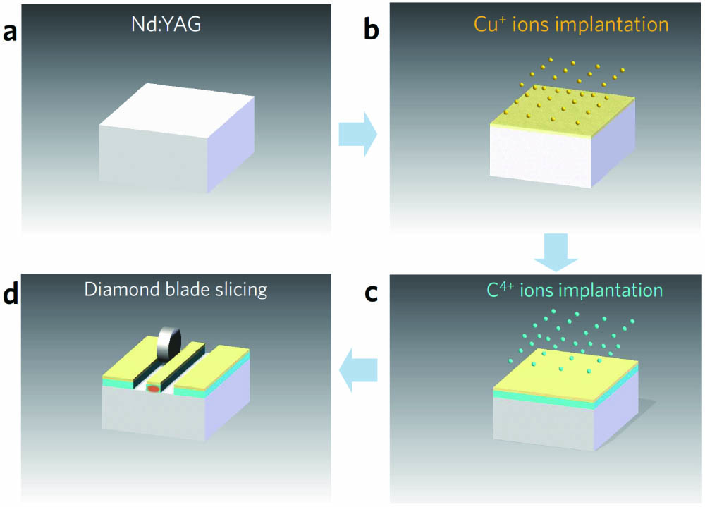
Copper (Cu) nanoparticles (NPs) are synthesized under the near-surface region of the (Nd:YAG) crystal by direct ions implantation. Subsequently, the monolithic ridge waveguide with embedded Cu NPs is fabricated by ions irradiation and diamond saw dicing. The nonlinear optical response of the sample is investigated by the Z-scan technique, and pronounced saturable absorption is observed at the 1030 nm femtosecond laser. Based on the obvious saturable absorption of Cu NPs embedded Nd:YAG crystal, 1 μm monolithic mode-locked pulsed waveguide laser is implemented by evanescent field interaction between NPs and waveguide modes, reaching the pulse duration of 24.8 ps and repetition rate of 7.8 GHz. The work combines waveguides with NPs, achieving pulsed laser devices based on monolithic waveguide chips.
waveguide lasers nanoparticles localized surface plasmon resonance saturable absorption Chinese Optics Letters
2021, 19(2): 021301
1 中国科学院上海光学精密机械研究所空间激光信息传输与探测技术重点实验室, 上海 201800
2 中国科学院大学, 北京 100049
平面波导激光器是板条激光器与光纤激光器的良好结合体, 其结合了两者的优点且避免了各自的缺点, 极高的宽高比率使流经工作区的一维梯度热流控制了热透镜效应, 同时对横向光束质量具有良好的控制; 通过增加工作区的宽和长可以增大输出功率, 大发散角的抽运光可以被约束在大数值孔径的波导结构中, 激光亮度极高。介绍了平面波导激光器的制备与材料以及发展, 综述了已报道的平面波导激光器相关研究, 并展望了其未来的发展。
激光器 全固态激光器 平面波导激光器 进展 激光与光电子学进展
2017, 54(5): 050004


