Author Affiliations
Abstract
1 Soochow University, Institute of Functional Nano and Soft Materials (FUNSOM), Jiangsu Key Laboratory for Carbon-Based Functional Materials and Devices, Suzhou, China
2 Soochow University, College of Chemistry, Chemical Engineering and Materials Science, Jiangsu Engineering Laboratory of Novel Functional Polymeric Materials, Suzhou, China
3 Macau University of Science and Technology, Macao Institute of Materials Science and Engineering, Macau, China
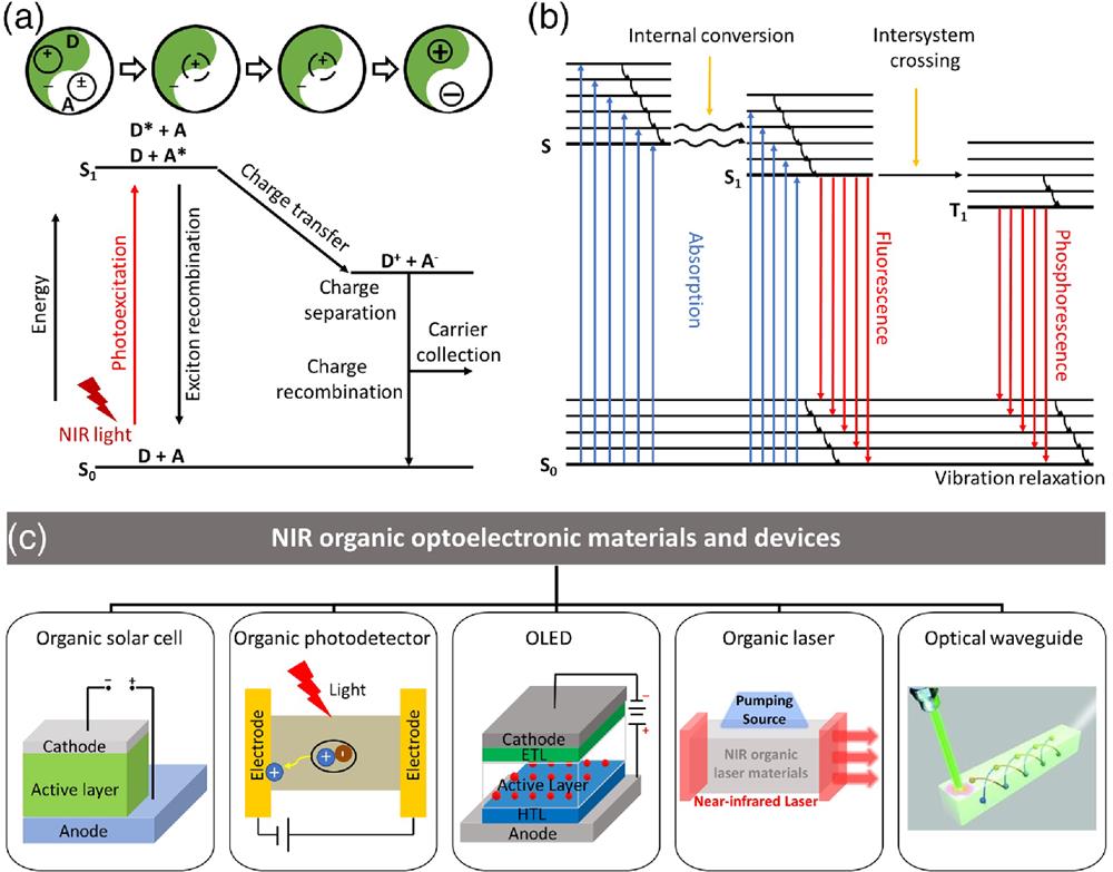
Near-infrared (NIR) light has shown great potential for military and civilian applications owing to its advantages in the composition of sunlight, invisibility to human eyes, deeper penetration into biological tissues, and low optical loss in optical fibers. Therefore, organic optoelectronic materials that can absorb or emit NIR light have aroused great scientific interest in basic science and practical applications. Based on these NIR organic optoelectronic materials, NIR optoelectronic devices have been greatly improved in performance and application. In this review, the representative NIR organic optoelectronic materials used in organic solar cells, organic photodetectors, organic light-emitting diodes, organic lasers, and organic optical waveguide devices are briefly introduced, and the potential applications of each kind of device are briefly summarized. Finally, we summarize and take up the development of NIR organic optoelectronic materials and devices.
near-infrared organic optoelectronic materials organic solar cells organic light-emitting devices organic optical waveguides Advanced Photonics
2024, 6(1): 014001
1 北京大学物理学院 介观物理国家重点实验室,纳光电子前沿科学中心,北京 100871
2 北京量子信息科学研究院,北京 100193
3 中国科学院物理研究所 北京凝聚态物理国家研究中心,北京 100190
由于量子限制效应,自组装半导体单量子点具有类似于原子的分立能级,可实现高不可分辨、高亮度和高纯度的单光子发射,其多种激子态能够产生不同偏振模式的光子。而光学微纳结构是调控量子点发光性质的有效手段,当单个量子点与光学微腔发生弱耦合时,Purcell效应将大大提高量子点作为单光子源或纠缠光子对源的性能。同时,量子点与光学微腔的强耦合系统可以作为量子光学网络中的量子节点,以及用于研究单光子水平的光学非线性效应。利用量子点与光学波导的耦合可实现固态量子比特和飞行光子比特的相干转换,以及高效的信息处理与传输,由此构建可靠的片上光学网络。此外,单量子点还具有可操控的自旋态,可作为量子比特的载体。考虑到量子点器件的制备过程易与成熟的半导体技术相结合,基于量子点的器件设计具有良好的可扩展性和集成化潜力。
自组装半导体量子点 激子 自旋 光学微腔 光波导 self-assembled semiconductor quantum dots excitons spins optical microcavities optical waveguides 
Author Affiliations
Abstract
This paper presents the development of a bioinspired multifunctional flexible optical sensor (BioMFOS) as an ultrasensitive tool for force (intensity and location) and orientation sensing. The sensor structure is bioinspired in orb webs, which are multifunctional devices for prey capturing and vibration transmission. The multifunctional feature of the structure is achieved by using transparent resins that present both mechanical and optical properties for structural integrity and strain/deflection transmission as well as the optical signal transmission properties with core/cladding configuration of a waveguide. In this case, photocurable and polydimethylsiloxane (PDMS) resins are used for the core and cladding, respectively. The optical transmission, tensile tests, and dynamic mechanical analysis are performed in the resins and show the possibility of light transmission at the visible wavelength range in conjunction with high flexibility and a dynamic range up to 150 Hz, suitable for wearable applications. The BioMFOS has small dimensions (around 2 cm) and lightweight (0.8 g), making it suitable for wearable application and clothing integration. Characterization tests are performed in the structure by means of applying forces at different locations of the structure. The results show an ultra-high sensitivity and resolution, where forces in the μN range can be detected and the location of the applied force can also be detected with a sub-millimeter spatial resolution. Then, the BioMFOS is tested on the orientation detection in 3D plane, where a correlation coefficient higher than 0.9 is obtained when compared with a gold-standard inertial measurement unit (IMU). Furthermore, the device also shows its capabilities on the movement analysis and classification in two protocols: finger position detection (with the BioMFOS positioned on the top of the hand) and trunk orientation assessment (with the sensor integrated on the clothing). In both cases, the sensor is able of classifying the movement, especially when analyzed in conjunction with preprocessing and clustering techniques. As another wearable application, the respiratory rate is successfully estimated with the BioMFOS integrated into the clothing. Thus, the proposed multifunctional device opens new avenues for novel bioinspired photonic devices and can be used in many applications of biomedical, biomechanics, and micro/nanotechnology.This paper presents the development of a bioinspired multifunctional flexible optical sensor (BioMFOS) as an ultrasensitive tool for force (intensity and location) and orientation sensing. The sensor structure is bioinspired in orb webs, which are multifunctional devices for prey capturing and vibration transmission. The multifunctional feature of the structure is achieved by using transparent resins that present both mechanical and optical properties for structural integrity and strain/deflection transmission as well as the optical signal transmission properties with core/cladding configuration of a waveguide. In this case, photocurable and polydimethylsiloxane (PDMS) resins are used for the core and cladding, respectively. The optical transmission, tensile tests, and dynamic mechanical analysis are performed in the resins and show the possibility of light transmission at the visible wavelength range in conjunction with high flexibility and a dynamic range up to 150 Hz, suitable for wearable applications. The BioMFOS has small dimensions (around 2 cm) and lightweight (0.8 g), making it suitable for wearable application and clothing integration. Characterization tests are performed in the structure by means of applying forces at different locations of the structure. The results show an ultra-high sensitivity and resolution, where forces in the μN range can be detected and the location of the applied force can also be detected with a sub-millimeter spatial resolution. Then, the BioMFOS is tested on the orientation detection in 3D plane, where a correlation coefficient higher than 0.9 is obtained when compared with a gold-standard inertial measurement unit (IMU). Furthermore, the device also shows its capabilities on the movement analysis and classification in two protocols: finger position detection (with the BioMFOS positioned on the top of the hand) and trunk orientation assessment (with the sensor integrated on the clothing). In both cases, the sensor is able of classifying the movement, especially when analyzed in conjunction with preprocessing and clustering techniques. As another wearable application, the respiratory rate is successfully estimated with the BioMFOS integrated into the clothing. Thus, the proposed multifunctional device opens new avenues for novel bioinspired photonic devices and can be used in many applications of biomedical, biomechanics, and micro/nanotechnology.
optical sensors optical waveguides bioinspired design multifunctional structures wearable sensors Opto-Electronic Advances
2022, 5(10): 210098

Author Affiliations
Abstract
1 Qingdao University, College of Physics Science, Center for Marine Observation and Communications, Qingdao, China
2 Shandong University, School of Physics, State Key Laboratory of Crystal Materials, Jinan, China
Femtosecond laser inscription or writing has been recognized as a powerful technique to engineer various materials toward a number of applications. By efficient modification of refractive indices of dielectric crystals, optical waveguides with diverse configurations have been produced by femtosecond laser writing. The waveguiding properties depend not only on the parameters of the laser writing but also on the nature of the crystals. The mode profile tailoring and polarization engineering are realizable by selecting appropriate fabrication conditions. In addition, regardless of the complexity of crystal refractive index changes induced by ultrafast pulses, several three-dimensional geometries have been designed and implemented that are useful for the fabrication of laser-written photonic chips. Some intriguing devices, e.g., waveguide lasers, wavelength converters, and quantum memories, have been made, exhibiting potential for applications in various areas. Our work gives a concise review of the femtosecond laser-inscribed waveguides in dielectric crystals and focuses on the recent advances of this research area, including the fundamentals, fabrication, and selected photonic applications.
femtosecond laser writing femtosecond laser inscription optical waveguides dielectric crystals laser crystals nonlinear optical crystals waveguide lasers frequency/wavelength conversion quantum photonic chip quantum memories Advanced Photonics
2022, 4(2): 024002
School of Optical and Electronic Information, Wuhan National Laboratory for Optoelectronics, Huazhong University of Science and Technology, Wuhan 430074, China
Optical traps have emerged as powerful tools for immobilizing and manipulating small particles in three dimensions. Fiber-based optical traps (FOTs) significantly simplify optical setup by creating trapping centers with single or multiple pieces of optical fibers. In addition, they inherit the flexibility and robustness of fiber-optic systems. However, trapping 10-nm-diameter nanoparticles (NPs) using FOTs remains challenging. In this study, we model a coaxial waveguide that works in the optical regime and supports a transverse electromagnetic (TEM)-like mode for NP trapping. Single NPs at waveguide front-end break the symmetry of TEM-like guided mode and lead to high transmission efficiency at far-field, thereby strongly altering light momentum and inducing a large-scale back-action on the particle. We demonstrate, via finitedifference time-domain (FDTD) simulations, that this FOT allows for trapping single 10-nm-diameter NPs at low power.
fiber-based optical trap (FOT) optical waveguides optical apertures metal nanophotonic structures self-induced back-action plasmonic optical trapping Frontiers of Optoelectronics
2021, 14(4): 399–406
天津大学精密仪器与光电子工程学院, 天津 300072
相较于电神经网络,光神经网络有着速度快、功耗低等优点,逐渐引起了人们的研究兴趣。光蓄水池神经网络是光循环神经网络的一种,适用于处理时序数据,对网络的训练过程比较简单。介绍了蓄水池神经网络的架构、特点以及实现蓄水池需要满足的条件。从具体硬件入手,以串行结构和并行结构两种构建方式进行分类,介绍了光蓄水池神经网络的研究进展。最后分析了当前光蓄水池神经网络存在的问题以及解决方案,并对其未来发展进行了展望。
中国激光
2021, 48(19): 1906001
Author Affiliations
Abstract
National Laboratory of Solid State Microstructures, College of Engineering and Applied Sciences, and School of Physics, Nanjing University, Nanjing 210093, China
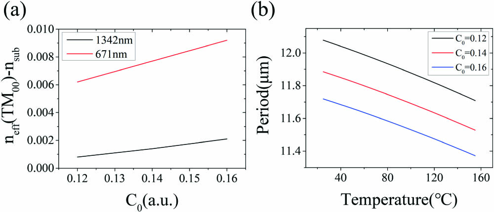
We report efficient generation of 671 nm red light based on quasi-phase-matched second harmonic generation of 1342 nm in LiNbO3 waveguides. The design method and fabrication process of the high-quality annealed proton-exchanged periodically poled channel waveguides were presented. A continuous-wave 1.71 mW red light was obtained with a single-pass conversion efficiency of 47%·W-1·cm-2, which is 88% that of the theoretical value. While for 1 mW quasi-continuous-laser input, the corresponding peak power being 2 W, the conversion efficiency reached up to 60%. Our results indicate that the annealed proton-exchanged periodically poled LiNbO3 waveguide is promising for high-efficiency and low power consumption nonlinear generation of visible light.
lithium niobate second-harmonic generation optical waveguides proton exchange Chinese Optics Letters
2020, 18(11): 111902


