Plasmonic evolution maps for planar metamaterials  Download: 717次
1. INTRODUCTION
Over the past decade, planar metamaterials that act as two-dimensional single-layer counterparts to fully three-dimensional metamaterials have drawn intense attention [1–4]. As compared to three-dimensional metamaterials, planar metamaterials are considerably simpler in terms of fabrication by top-down techniques. In addition to a negative refractive index, which is the most remarkable property of metamaterials [5], many other attractive phenomena for condensed-state and quantum-classical analogies have been reported in planar metamaterials. These phenomena include the Fano resonance [6,7], the electromagnetically induced transparency [8–10], near-zero refractive index [11,12], and the topological edge states [13–15]. From the microwave range to the terahertz, infrared, and optical ranges, a variety of planar metamaterials have been designed and applied in perfect absorber [16], sensing [17,18], circular dichroism [19–21], wave plates [22–24], coherent modulation [25,26], electrical modulators [27–34], metalenses [35–38], and optical rulers [39].
Accompanying this fast development, the underlying theoretical methods always play a fundamental role in designing planar metamaterials with particular phenomena and applications. Considering that the unit cell of a planar metamaterial is usually made of a plasmonic atom or molecule, it becomes critical to understand the mode’s origin and features during the analysis. Some classical electromagnetic analysis theories and methods, such as the Mie theory [40], the coupled-mode theory [9,41], the multipole-expansion method [42,43], and the inductive-capacitive (LC) equivalent-circuit model [44], have been widely applied to predict the resonant modes of simple planar metamaterials. For complex structures, the electromagnetic simulation tools, such as the finite-element method [18–21,27–33], the finite-difference time-domain method [9,11,16,17,35–38], and the moment method [45], have become more universal for verifying a mode’s wavelength and features. In addition, Rechberger et al. and Prodan et al. have established particular plasmonic hybridization models (PHMs) to well describe the mode coupling and energy states in complex plasmonic molecules [46–49].
In many studies, mode analysis directly based on the final field/charge/current distribution is simple and efficient for us to identify a mode’s type and order in simple plasmonic atoms, such as nanodisks [11], nanorods [35], and L-shaped nanostructures [24]. However, for more complex plasmonic atoms, such as square rings [50], split-ring resonators [27–33], H-shaped nanostructures [51], and S-shaped nanostructures [23], it is difficult to deeply understand a mode’s origin because the final field/charge/current distribution does not reveal the complicated formation process of a plasmonic mode. Based on the PHM, we can efficiently and clearly understand the coupling mechanism of low-order modes in plasmonic molecules [47–49,52–55]. However, such a model will become less efficient or even invalid for high-order modes in a plasmonic molecule constructed by complex plasmonic atoms.
Considering the above issues, in this paper, we would like to propose a new analysis method based on natural evolution theory in order to understand the modes’ origin and coupling mechanism in planar metamaterials constructed by complex plasmonic atoms and molecules. We assume that a complex plasmonic atom/molecule initially grows from one basic element, and introduce several structural and mode evolution operators to construct evolutional maps that can well describe the modes’ formation process. We will also clearly reveal the dependency of a structure’s symmetry on the formation of a plasmonic mode based on our proposed mode evolution method (MEM).
2. RESULTS
2.1 A. Planar Metamaterial Samples
We consider two typical complex planar metamaterials in our study, i.e., the complementary split-ring resonator (CSRR) and the H-shaped air slit. As shown in Fig. 1(a), the CSRR contains a square air ring with one or more splits on the upper/bottom sides of the air ring. The side length and the slit width of the square air ring are defined as and , respectively. The width of split is denoted as , and represents the horizontal displacement of the split from the center. In the experiment, six CSRR planar metamaterial samples with different values for the split number and symmetry were fabricated. A 50-nm thick gold layer was first deposited on the glass substrate by thermal evaporation (Oerlikon Univex 250). The patterns of CSRR planar metamaterials were then transferred onto the gold layer by using focused ion beam milling (FEI Helios NanoLab 650). It can be seen from the scanning electron microscope (SEM) images that all of the samples have high quality, with good homogeneity and consistency [Fig. 1(b)]. The structural parameters of these samples are approximately , , and . The period of each array is 625 nm in both the and directions. Sample I without any split was fabricated for comparison purposes. Sample II and Sample III have one split at the upper center () and the upper right side (), respectively. Sample IV, Sample V, and Sample VI have two splits at the upper and bottom sides of the air ring with different values of . As far as the mirror and center inversion symmetries are concerned, Sample I and Sample IV satisfy both the mirror and center inversion symmetries, while Sample II and Sample VI satisfy only the mirror symmetry and the center inversion symmetry, respectively. Sample III and Sample V show neither mirror nor center inversion symmetry.
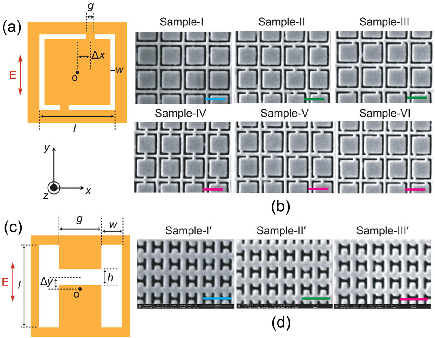
Fig. 1. Schematic diagram and SEM images of the (a), (b) CSRR and (c), (d) H-shaped complementary planar metamaterials. From Sample I to Sample VI, different numbers of splits are introduced and arranged in designed symmetry/asymmetry.
For the H-shaped air slit, the length and the width of the vertical air slits are defined as and , and the length and width of the horizontal air slit are defined as and , respectively [Fig. 1(c)]. A vertical displacement for the horizontal air slit is introduced along the vertical direction. As indicated by Fig. 1(d), we fabricated three H-shaped air slit planar metamaterial samples with different values of , i.e., Sample (), Sample (), and Sample (). The period of each array is 305 nm in both the and directions, and the other structural parameters are approximately , , , and . Sample satisfies the mirror symmetry and center inversion symmetry, while Sample and Sample have only mirror symmetry.
2.2 B. Reflection Spectra and Conventional Mode Analysis
The reflection spectra of the samples were measured with a visible-near-infrared microspectrophotometer (Jasco MSV-5200). A commercial software package, Lumerical FDTD Solutions, was used to simulate the reflection spectra of samples. In our simulation, the plane wave source was used to excite the eigenmodes of planar metamaterials. The periodic boundary condition was used along the and directions, and the perfectly matched layer (PML) absorbing boundary condition was used along both the directions. The grid size was set as 2 nm for the , , and directions. The complex permittivity of the gold was fitted to the Johnson and Christy data.
Figure 2 shows the experimental and simulated reflection spectra of the CSRR samples when the light is normally incident to the metamaterials with an electric field polarized along the direction. The experimental spectra match well with the simulation spectra in terms of the resonance number and location. It is found that the resonance number has a close relationship with the symmetry of the CSRRs. Specifically speaking, Sample I, which has the highest symmetry, shows two main resonances in the near-infrared band [Fig. 2(a)]. One resonance is located at 1057 nm (I-1). Another resonance located at around 3200 nm is not shown here due to the spectrum limit in the experiment. When one split is introduced without displacement (), the horizontal symmetry of the square air ring is broken, and we can observe three resonances (II-1 at 999 nm, II-2 at 1295 nm, and II-3 at 2165 nm) in the spectra of Sample II [Fig. 2(b)]. For Sample III, with a positive displacement of 150 nm, both the horizontal and vertical symmetries of the square air ring are broken, and there is one more minor resonance (III-4 at 1221 nm) in the spectra [Fig. 2(c)]. In comparison, when two splits without displacement are introduced in Sample IV, both the horizontal and vertical symmetries are recovered, and the resonance number is reduced to two again [Fig. 2(d)]. Similar to Sample III, Sample V also shows four resonances due to the completely broken horizontal and vertical symmetries [Fig. 2(e)]. The last sample, Sample VI, only has a center inversion symmetry, but its reflection spectra are similar to those of Sample IV, which also satisfies the center inversion symmetry [Fig. 2(f)]. Actually, more symmetry breaking of CSRRs usually corresponds to more resonances because high-order modes prefer to stay in the low-symmetry structures [56–58]. It should be noted that when the plane wave is polarized along the direction, the resonances are also sensitive to the symmetries of the six CSRR samples. The relation between resonance and structural symmetry is similar to the -polarization case.
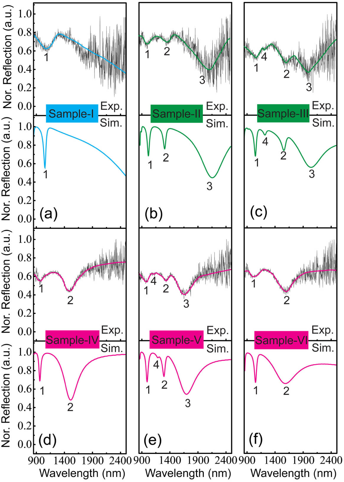
Fig. 2. Experimental and simulated reflection spectra of (a) Sample I, (b) Sample II, (c) Sample III, (d) Sample IV, (e) Sample V, and (f) Sample VI. The solid curve in each experimental spectrum serves as a guide for easier comparison.
One conventional method for the mode analysis of SRRs/CSRRs is simulating the final electric field and charge distributions of resonant modes. From Figs. 3(a), 3(d), 3(g), and 3(j), it is clear to see that the electric-field amplitude distribution of the representative modes in Fig. 2 retains the structural symmetry of the samples well. The higher-order mode contains more subregions with concentrated electric fields. Based on the corresponding charge distribution, as presented in Figs. 3(b), 3(e), 3(h), and 3(k), II-5 and III-5 show a clear dipole-like charge distribution, and the higher-order modes show more pairs of dipole-like charges. However, it is difficult to understand the modes’ origin of these higher-order modes based on the final electric field and charge distributions.
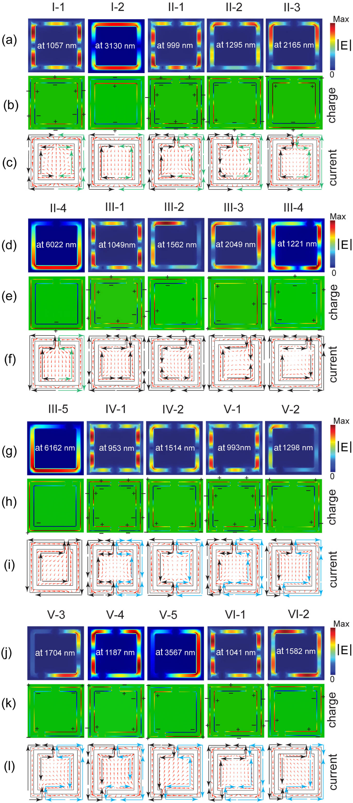
Fig. 3. Conventional mode analysis for Samples I–VI. (a), (d), (g), (j) Electric field distributions; (b), (e), (h), (k) charge distributions; (c), (f), (i), (l) current distributions. The big arrows serve as a guide to show the current directions at the metal/air surface. The symmetrically distributed currents in the plasmonic atom samples (I–III) are highlighted by green color, and the currents in the right atom of the plasmonic molecule samples (IV–VI) are highlighted by blue color.
Another widely used method is using an LC equivalent-circuit model to predict the resonant modes of SRRs/CSRRs [44]. In particular, the resonant frequency of the fundamental LC mode is written as , where and are the effective inductance and capacitance, respectively. According to the Babinet principle [59], CSRRs work as dual SRRs. In our study, light is normally incident to the samples, and the electric moments associated with the induced currents are perpendicular to the plane of the CSRRs. Therefore, the interaction of the induced electric moments with the electric field of the incident wave is negligible, while the circulating surface current distribution is generally used to identify the possible LC resonance in the CSRRs [60]. As shown in Figs. 3(c), 3(f), 3(i), and 3(l), II-5 and III-5 are proposed to originate from the fundamental LC resonance because the light can drive a couple of circulating surface currents in the split of each CSRR unit cell. The current flows become more complex for the higher-order modes, and it is difficult to identify these modes based on the LC model.
Figures 4(a) and 4(b) show the experimental and simulated reflection spectra for three H-shaped air slit planar metamaterial samples when the plane wave is polarized along the direction. Sample is a symmetrical structure with only one resonance located at 1446 nm. Sample shows a new resonance at 889 nm when its vertical symmetry is broken. As vertical symmetry is further broken in Sample , the additional resonance at 837 nm is enhanced with a slight blueshift. The corresponding electric-field and charge distributions of resonant modes are given in Figs. 4(c) and 4(d). It is clear to see that the electric field of mode is concentrated in the horizontal air slit and mode contains three pairs of dipole-like charges. For , in addition to the concentrated electric field in the horizontal air slit, we can also observe “hot spots” at the lower corners that connect the horizontal and vertical air slits. For , only hot spots are found near the upper corners. Both and contain three pairs of dipole-like charges with different charge distributions. More distinct hot spots can be observed from and when the vertical symmetry is further broken. It is difficult to understand the origin of these modes based on the final electric field and charge distributions. From the surface current distributions in Fig. 4(e), the modes , , and are proposed to originate from the fundamental LC resonance because the light can drive a couple of circulating surface currents in the gap of two vertical slits. This LC resonance is less influenced by the vertical displacement of the horizontal air slit because the total length of the circulating surface currents is not changed. The higher-order modes, however, are also difficult to be identified based on the LC model. When the plane wave is polarized along the direction, the resonances are almost not influenced by the vertical displacement of the horizontal air slit.
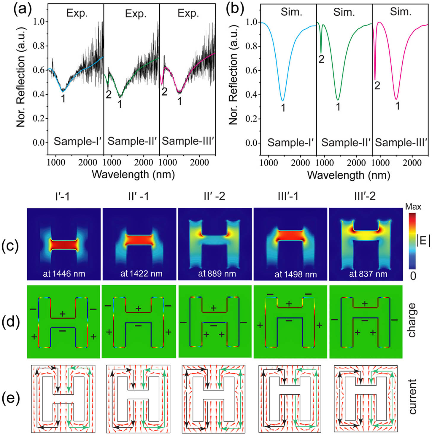
Fig. 4. Conventional mode analysis for three H-shaped complementary planar metamaterials. (a), (b) Experimental and simulated reflection spectra; (c) electric field distributions; (d) charge distributions; (e) current distributions. The symmetrically distributed currents are highlighted by green color.
2.3 C. Mode Analysis Based on PEMs
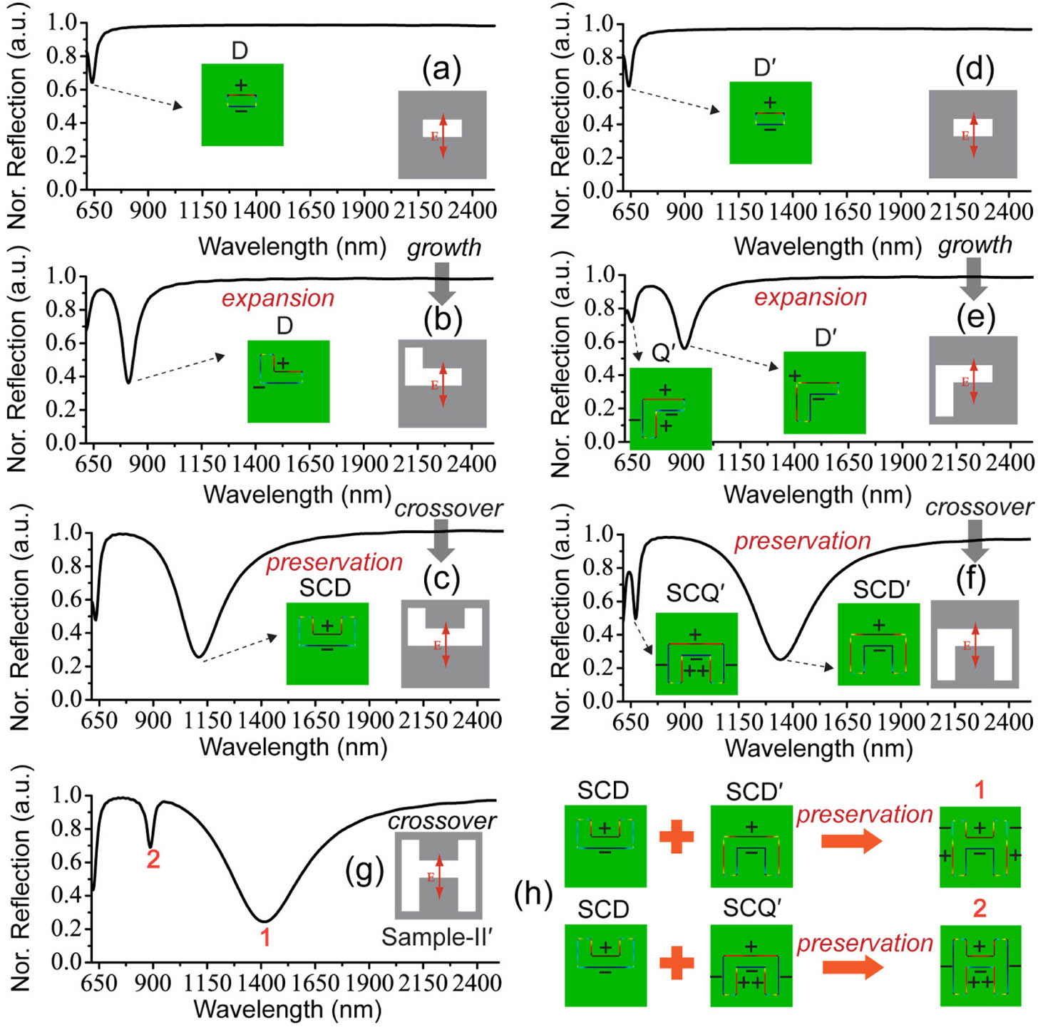
The above mode analysis based on conventional methods shows obvious limitations for deeply understanding the modes’ origin in complex planar metamaterials. Here we propose a new method called the MEM with a core analysis tool, i.e., plasmonic evolution maps (PEMs) in order to give a qualitative explanation of the modes’ origin. The PEMs contain three elements, i.e., structural operator, mode operator, and characteristic spectra/charge distribution. In the following contents, we will illustrate how the PEMs work for different plasmonic atom samples (Samples I–III and Samples ) and plasmonic molecule samples (Samples IV–VI).
Figures 5(a)–5(d) present the PEMs for Sample I, which gradually grows from a horizontal air slit (primary state) into the square air ring (final state). The structural operators during the evolutional process include growth and crossover, while the related structural operators include expansion, preservation, and mutation. From Fig. 5(a), we can see that the primary horizontal air slit shows only one dipole-like resonance at 1612 nm. When the L-shaped air slit is constructed via the structural operator growth, besides the dipole-like resonance at 3205 nm, it can support two additional higher-order plasmonic modes due to the increased air slit’s length, i.e., a quadrupole-like charge at 1716 nm and a hexapole-like charge at 1107 nm [Fig. 5(b)]. It should be noted that these higher-order modes are not real electric quadrupoles or hexapoles. They are actually the higher-order surface plasmon polariton (SPP) modes that satisfy the standing-wave formula , where is the total length of the air slit, is the effective refractive index of the SPP waveguide, and is the order of eigenmode. For the L-shaped air slit with a length of 1100 nm, the calculated eigenmodes are located at 3410 nm (, ), 1705 nm (, ), and 1173 nm (, ), which are close to the simulation results. As a result, a mode operator expansion is defined to describe the mode evolution during the growth of the structure. Under expansion operation, the quantity of the mode is continuously increasing and the mode’s order clearly depends on how many pairs of electric dipoles it has.
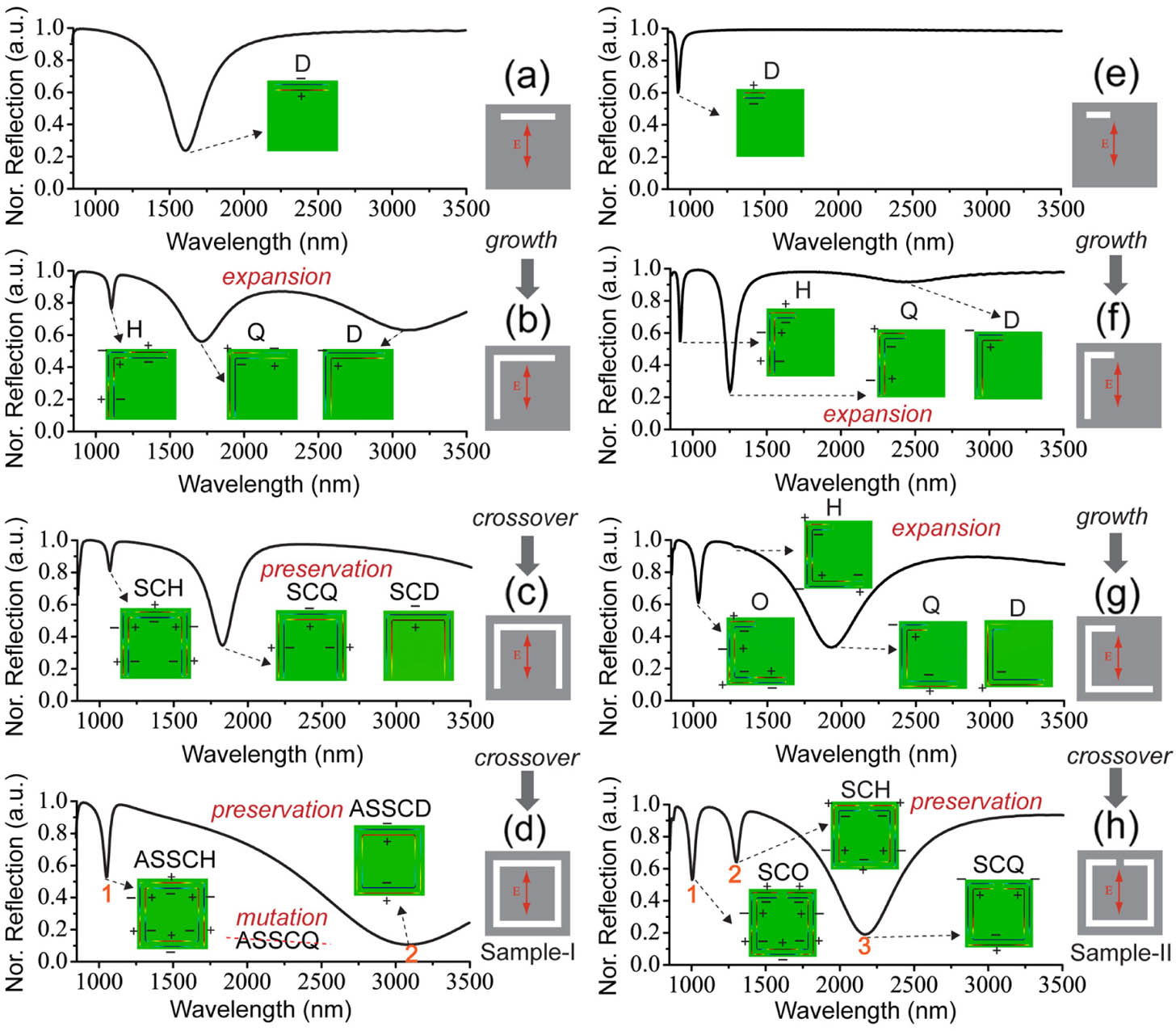
Fig. 5. Mode analysis based on PEMs for (a)–(d) Sample I and (e)–(h) Sample II. D, dipole-like; Q, quadrupole-like; H, hexapole-like; O, octopole-like charge distributions; SCD/SCQ/SCH/SCO, symmetrically coupled dipole-like/quadrupole-like/hexapole-like/octopole-like charge distributions; ASSCD/ASSCQ/ASSCH, antisymmetrically coupled SCD/SCQ/SCH modes.
When the L-shaped air slit further connects with a vertical air slit on the right side, the formed U-shaped air slit shows 10 pole-like, hexapole-like, and dipole-like charge distributions at 1052, 1794, and 4688 nm, respectively [Fig. 5(c)]. This L-U formation does not belong to a growth process because the number of dipolar pairs of three modes is not continuous. In fact, the 10 pole-like and hexapole-like charge distributions are symmetrically coupled hexapole-like (SCH) and symmetrically coupled quadrupole-like (SCQ) charge distributions considering that the U-shaped air slit possesses mirror symmetry, and the driving electric field shows symmetric polarization along the direction. The real mode order for SCH and SCQ is and , respectively. In other words, the SCH/SCQ in the U-shaped air slit (child structure) can be regarded as the overlapping (crossover) result of the two symmetric hexapole-like/quadrupole-like charge distributions in the left and right L-shaped air slits (parent structures). As a result, a mode operator preservation is defined to describe the mode evolution during the crossover of the structure. The preservation operation means that the child structure retains the same or similar genes (charge distributions) of the parent structures and that its charge distribution is the internal overlapping result of the parent structures after crossover. The preservation operation may narrow the linewidth of the eigenmode (such as SCQ).
The final square air ring can be regarded as the second-generation child structure of two parent U-shaped air slits after crossover [Fig. 5(d)]. Considering that the square air ring possesses mirror symmetry and the driving electric field shows antisymmetric polarization along the direction, resonances 1 and 2 are actually the antisymmetrically coupled SCH (ASSCH) and antisymmetrically coupled SCD (ASSCD) modes, respectively. Under the preservation operation, the ASSCH mode shows an enhanced line shape compared to the SCH mode due to the constructive coupling along the vertical air slits, while the ASSCD mode (two parallel short dipoles) shows a great blueshift with respect to the SCD mode (a long dipole) due to the destructive coupling along the vertical air slits. In particular, there is no antisymmetrically coupled SCQ (ASSCQ) in the spectrum due to the destructive coupling between two antisymmetric SCQ modes along the vertical air slits. This missing mode phenomenon behaves like a mutation in the evolution process. Therefore, a mode operator mutation is defined to describe the unpreserved charge distributions during the crossover.
Figures 5(e)–5(h) present the PEMs for Sample II. As compared to the square air ring, this CSRR with one split shows two main different points during the mode evolution. One difference is that the L-U formation still belongs to the growth process because the mode’s quantity is further increased and the mode’s order is still continuous from Figs. 5(f) and 5(g). Another difference is that the mutation operation is absent during the crossover process of two asymmetrical U-shaped air slits arranged in a mirror symmetry [Fig. 5(h)]. Due to completely broken symmetry, the mode evolution of Sample III always belongs to the growth process from the primary state to the final state.
Figure 6 presents the PEMs for Sample , which can be divided into two back-to-back U-shaped air slits. For the upper U-shaped air slit, a dipole-like charge evolutional process (D-SCD) can be observed [Figs. 6(a)–6(c)], while the lower U-shaped air slit corresponds to both dipole () and quadrupole-like charge () evolutional processes [Figs. 6(d)–6(f)]. The formations of SCD, , and modes in Sample are similar to those in Figs. 5(a)–5(c). As shown in Fig. 6(g), the final resonances 1 and 2 of the H-shaped air slit are the crossover results of the upper and lower U-shaped air slits. Based on the charge distribution in Fig. 6(h), resonances 1 and 2 are the combination of and via the preservation operation, respectively. The PEMs for Sample and Sample are similar to those of Sample .
For Sample IV, Sample V, and Sample VI, which are plasmonic molecule samples, we define a structural operator (group) and two mode operators (preservation and learning) to describe the mode evolution in the plasmonic molecules. Preservation means that the charge distribution of each plasmonic atom keeps unchanged when they are combined in a group. Learning means that the charge distribution of a plasmonic atom in the group is affected by neighboring atoms. As shown in Fig. 7(a), for Sample V, resonance 1 is the preservation result of modes L1 and R1, while resonances 2 and 3 are the learning results from modes L2 and R2 by comparing with the charge distributions at the square and circle positions. As a comparison, the resonances of Sample VI, which contains the same two plasmonic atoms arranged in center inversion symmetry, are all due to the preservation operation during the group process [Fig. 7(b)]. The PEMs for Sample IV, which contains the same two plasmonic atoms arranged in mirror symmetry, are similar to Sample VI. This is because the atoms in Sample IV and Sample VI have the same order eigenmodes due to a fixed total length, and the mode preservation during the crossover and group processes does not change the number and resonant position of eigenmodes.
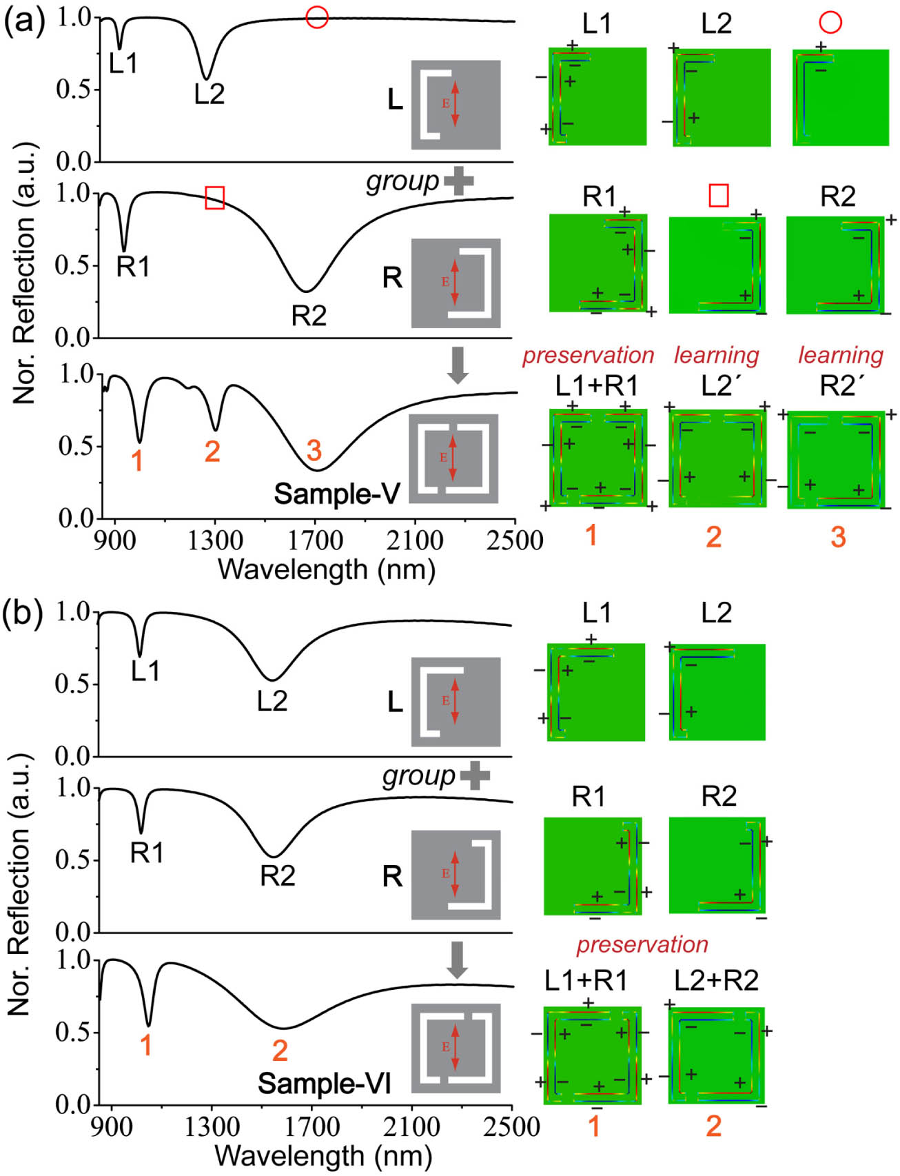
Fig. 7. Mode analysis based on PEMs for (a) Sample V and (b) Sample VI. The square and circle in (a) correspond to the positions of modes 2 and 3, respectively.
Based on these PEMs for plasmonic atom and molecule samples, it is found that the use of structural and mode operators strongly depends on the structural symmetry of samples. The physical mechanism behind the mode operators includes the near- or far-field excitation of plasmonic modes as well as the intrinsic or external coupling between plasmonic modes. The PEMs and the related mechanism construct the MEM for mode analysis in the plasmonic atoms and molecules, as summarized in Table 1.
Table 1. Summarization of MEM for Plasmonic Atoms and Molecules
|
3. DISCUSSION AND CONCLUSION
For a particular plasmonic atom or molecule, how to construct suitable PEMs is very important for the application of the MEM. General guidance for this issue is given as follows. First, the PEMs of a plasmonic molecule are fixed via the group of constituted plasmonic atoms. Second, the PEMs of a constituted plasmonic atom start from the growth process based on a primary state. If the intermediate state of the plasmonic atom shows a structural symmetry or the continuity of the mode’s order is broken, the growth process should be terminated and replaced by the crossover process. Third, the choice of primary and intermediate states is not fixed, and thus a constituted plasmonic atom may have different PEMs. For instance, the PEMs of Sample can be constructed following the sequence of either L-U-H or L-T-H. Both of them can explain the final resonant modes well with different coupling mechanisms. Based on the above guidance, we have successfully verified the PEMs for other typical planar metamaterials, including the S-shaped planar metamaterial [23], the electric CSRR [29], and the hybrid CSRR [61]. In addition to the complementary planar metamaterials, the PEMs can also be applied for the normal type. For example, we have constructed the PEMs for the normal SRRs related to Sample I and Sample II and found that the SRRs show a one-to-one correspondence of plasmonic resonances to those of the CSRRs in Fig. 5. Therefore, the PEMs also satisfy the Babinet principle [59].
In principle, the MEM can be applied to arbitrary plasmonic atoms and molecules. For a plasmonic atom, the MEM works as a kind of ab initio theory applied in nanophotonics and plasmonics. For a plasmonic molecule, the MEM becomes a supplement to the widely used PHM, which contains one structural operator (“hybridization”) and two mode operators (“bonding” and “anti-bonding”), as well as a core analysis tool (energy-state maps). The PHM is mainly used among lower orders of plasmonic modes such as dipole–dipole and dipole–quadruple coupling [47–49,52–55], while there is no limitation to the mode’s order based on the MEM. A combination of the MEM and PHM is able to provide comprehensive mode analysis for complex metamaterials.
In addition to mode analysis, some other potential applications are expected based on the MEM. For instance, we can freely tailor the bright (superradiant) and dark (subradiant) modes according to the symmetry-dependent PEMs of different plasmonic atoms and molecules, which is helpful in further studies on the coherent Mie scattering, Fano resonance, and electromagnetically induced transparency. We can also design a genetic metasurface based on the MEM. A conventional metasurface usually deals with information based on the Berry phase change of plasmonic atoms [35–38]. In comparison, a genetic metasurface will deal with information by writing or reading the evolutional relationships of internal plasmonic atoms.
[1] N. I. Zheludev. The road ahead for metamaterials. Science, 2010, 328: 582-583.
[2] Y. M. Liu, X. Zhang. Metamaterials: a new frontier of science and technology. Chem. Soc. Rev., 2011, 40: 2494-2507.
[3] H. T. Chen, A. J. Taylor, N. F. Yu. A review of metasurfaces: physics and applications. Rep. Prog. Phys., 2016, 79: 076401.
[4] S. B. Glybovski, S. A. Tretyakov, P. A. Belov, Y. S. Kivshar, C. R. Simovski. Metasurfaces: from microwaves to visible. Phys. Rep., 2016, 634: 1-72.
[5] D. R. Smith, J. B. Pendry, M. C. K. Wiltshire. Metamaterials and negative refractive index. Science, 2004, 305: 788-792.
[6] U. Fano. The theory of anomalous diffraction gratings and of quasi-stationary waves on metallic surfaces (Sommerfeld’s waves). J. Opt. Soc. Am., 1941, 31: 213-222.
[7] B. Luk’yanchuk, N. I. Zheludev, S. A. Maier, N. J. Halas, P. Nordlander, H. Giessen, C. T. Chong. The Fano resonance in plasmonic nanostructures and metamaterials. Nat. Mater., 2010, 9: 707-715.
[8] N. Papasimakis, V. A. Fedotov, N. I. Zheludev, S. L. Prosvirnin. Metamaterial analog of electromagnetically induced transparency. Phys. Rev. Lett., 2008, 101: 253903.
[9] N. Liu, L. Langguth, T. Weiss, J. Kastel, M. Fleischhauer, T. Pfau, H. Giessen. Plasmonic analogue of electromagnetically induced transparency at the Drude damping limit. Nat. Mater., 2009, 8: 758-762.
[10] J. Q. Gu, R. Singh, X. J. Liu, X. Q. Zhang, Y. F. Ma, S. Zhang, S. A. Maier, Z. Tian, A. K. Azad, H. T. Chen, A. J. Taylor, J. G. Han, W. L. Zhang. Active control of electromagnetically induced transparency analogue in terahertz metamaterials. Nat. Commun., 2012, 3: 1151.
[11] Y. Li, S. Kita, P. Munoz, O. Reshef, D. I. Vulis, M. Yin, M. Loncar, E. Mazur. On-chip zero-index metamaterials. Nat. Photonics, 2015, 9: 738-743.
[12] H. C. Chu, Q. Li, B. B. Liu, J. Luo, S. L. Sun, Z. H. Hang, L. Zhou, Y. Lai. A hybrid invisibility cloak based on integration of transparent metasurfaces and zero-index materials. Light Sci. Appl., 2018, 7: 50.
[13] H. N. S. Krishnamoorthy, Z. Jacob, E. Narimanov, I. Kretzschmar, V. M. Menon. Topological transitions in metamaterials. Science, 2012, 336: 205-209.
[14] W. J. Chen, S. J. Jiang, X. D. Chen, B. C. Zhu, L. Zhou, J. W. Dong, C. T. Chan. Experimental realization of photonic topological insulator in a uniaxial metacrystal waveguide. Nat. Commun., 2014, 5: 5782.
[15] J. Cha, K. W. Kim, C. Daraio. Experimental realization of on-chip topological nanoelectromechanical metamaterials. Nature, 2018, 564: 229-233.
[16] N. I. Landy, S. Sajuyigbe, J. J. Mock, D. R. Smith, W. J. Padilla. Perfect metamaterial absorber. Phys. Rev. Lett., 2008, 100: 207402.
[17] X. L. Xu, B. Peng, D. H. Li, J. Zhang, L. M. Wong, Q. Zhang, S. J. Wang, Q. H. Xiong. Flexible visible-infrared metamaterials and their applications in highly sensitive chemical and biological sensing. Nano Lett., 2011, 11: 3232-3238.
[18] C. H. Wu, A. B. Khanikaev, R. Adato, N. Arju, A. A. Yanik, H. Altug, G. Shvets. Fano-resonant asymmetric metamaterials for ultrasensitive spectroscopy and identification of molecular monolayers. Nat. Mater., 2012, 11: 69-75.
[19] E. Hendry, T. Carpy, J. Johnston, M. Popland, R. V. Mikhaylovskiy, A. J. Lapthorn, S. M. Kelly, L. D. Barron, N. Gadegaard, M. Kadodwala. Ultrasensitive detection and characterization of biomolecules using superchiral fields. Nat. Nanotechnol., 2010, 5: 783-787.
[20] C. Wu, N. Arju, G. Kelp, J. A. Fan, J. Dominguez, E. Gonzales, E. Tutuc, I. Brener, G. Shvets. Spectrally selective chiral silicon metasurfaces based on infrared Fano resonances. Nat. Commun., 2014, 5: 3892.
[21] Y. Chen, J. Gao, X. D. Yang. Chiral metamaterials of plasmonic slanted nanoapertures with symmetry breaking. Nano Lett., 2018, 18: 520-527.
[22] Y. Zhao, A. Alu. Tailoring the dispersion of plasmonic nanorods to realize broadband optical meta-waveplates. Nano Lett., 2013, 13: 1086-1091.
[23] Y. J. Chiang, T. J. Yen. A composite-metamaterial-based terahertz-wave polarization rotator with an ultrathin thickness, an excellent conversion ratio, and enhanced transmission. Appl. Phys. Lett., 2013, 102: 011129.
[24] S. C. Jiang, X. Xiong, Y. S. Hu, Y. H. Hu, G. B. Ma, R. W. Peng, C. Sun, M. Wang. Controlling the polarization state of light with a dispersion-free metastructure. Phys. Rev. X, 2014, 4: 021026.
[25] M. Papaioannou, E. Plum, J. Valente, E. T. F. Rogers, N. I. Zheludev. Two-dimensional control of light with light on metasurfaces. Light Sci. Appl., 2016, 5: e16070.
[26] A. Xomalis, I. Demirtzioglou, E. Plum, Y. Jung, V. Nalla, C. Lacava, K. F. MacDonald, P. Petropoulos, D. J. Richardson, N. I. Zheludev. Fibre-optic metadevice for all-optical signal modulation based on coherent absorption. Nat. Commun., 2018, 9: 182.
[27] H. T. Chen, J. F. O’Hara, A. K. Azad, A. J. Taylor, R. D. Averitt, D. B. Shrekenhamer, W. J. Padilla. Experimental demonstration of frequency-agile terahertz metamaterials. Nat. Photonics, 2008, 2: 295-298.
[28] G. Scalari, C. Maissen, D. Turcinkova, D. Hagenmueller, S. De Liberato, C. Ciuti, C. Reichl, D. Schuh, W. Wegscheider, M. Beck, J. Faist. Ultrastrong coupling of the cyclotron transition of a 2D electron gas to a THz metamaterial. Science, 2012, 335: 1323-1326.
[29] F. Valmorra, G. Scalari, C. Maissen, W. Fu, C. Schoenenberger, J. W. Choi, H. G. Park, M. Beck, J. Faist. Low-bias active control of terahertz waves by coupling large-area CVD graphene to a terahertz metamaterial. Nano Lett., 2013, 13: 3193-3198.
[30] R. Degl’Innocenti, D. S. Jessop, Y. D. Shah, J. Sibik, J. A. Zeitler, P. R. Kidambi, S. Hofmann, H. E. Beere, D. A. Ritchie. Low-bias terahertz amplitude modulator based on split-ring resonators and graphene. ACS Nano, 2014, 8: 2548-2554.
[31] N. Dabidian, I. Kholmanov, A. B. Khanikaev, K. Tatar, S. Trendafilov, S. H. Mousavi, C. Magnuson, R. S. Ruoff, G. Shvets. Electrical switching of infrared light using graphene integration with plasmonic Fano resonant metasurfaces. ACS Photon., 2015, 2: 216-227.
[32] P. Q. Liu, I. J. Luxmoore, S. A. Mikhailov, N. A. Savostianova, F. Valmorra, J. Faist, G. R. Nash. Highly tunable hybrid metamaterials employing split-ring resonators strongly coupled to graphene surface plasmons. Nat. Commun., 2015, 6: 8969.
[33] O. Balci, N. Kakenov, E. Karademir, S. Balci, S. Cakmakyapan, E. O. Polat, H. Caglayan, E. Ozbay, C. Kocabas. Electrically switchable metadevices via graphene. Sci. Adv., 2018, 4: eaao1749.
[34] A. Chanana, X. J. Liu, C. Zhang, Z. V. Vardeny, A. Nahata. Ultrafast frequency-agile terahertz devices using methylammonium lead halide perovskites. Sci. Adv., 2018, 4: eaar7353.
[35] M. Khorasaninejad, W. T. Chen, R. C. Devlin, J. Oh, A. Y. Zhu, F. Capasso. Metalenses at visible wavelengths: diffraction-limited focusing and subwavelength resolution imaging. Science, 2016, 352: 1190-1194.
[36] S. M. Wang, P. C. Wu, V. C. Su, Y. C. Lai, C. H. Chu, J. W. Chen, S. H. Lu, J. Chen, B. B. Xu, C. H. Kuan, T. Li, S. N. Zhu, D. P. Tsai. Broadband achromatic optical metasurface devices. Nat. Commun., 2017, 8: 187.
[37] L. L. Huang, X. Z. Chen, H. Muhlenbernd, H. Zhang, S. M. Chen, B. F. Bai, Q. F. Tan, G. F. Jin, K. W. Cheah, C. W. Qiu, J. S. Li, T. Zentgraf, S. Zhang. Three-dimensional optical holography using a plasmonic metasurface. Nat. Commun., 2013, 4: 2808.
[38] G. X. Zheng, H. Muhlenbernd, M. Kenney, G. X. Li, T. Zentgraf, S. Zhang. Metasurface holograms reaching 80% efficiency. Nat. Nanotechnol., 2015, 10: 308-312.
[39] G. H. Yuan, N. I. Zheludev. Detecting nanometric displacements with optical ruler metrology. Science, 2019, 364: 771-775.
[40] G. Mie. Beiträge zur Optik trüber Medien, speziell kolloidaler Metallösungen. Ann. Phys., 1908, 330: 377-445.
[41] M. Kang, Y. D. Chong, H. T. Wang, W. R. Zhu, M. Premaratne. Critical route for coherent perfect absorption in a Fano resonance plasmonic system. Appl. Phys. Lett., 2014, 105: 223301.
[42] J. Petschulat, C. Menzel, A. Chipouline, C. Rockstuhl, A. Tunnermann, F. Lederer, T. Pertsch. Multipole approach to metamaterials. Phys. Rev. A, 2008, 78: 043811.
[43] L. Y. Jiang, T. T. Yin, A. M. Dubrovkin, Z. G. Dong, Y. T. Chen, W. J. Chen, J. K. W. Yang, Z. X. Shen. In-plane coherent control of plasmon resonances for plasmonic switching and encoding. Light Sci. Appl., 2019, 8: 21.
[44] J. D. Baena, J. Bonache, F. Martin, R. M. Sillero, F. Falcone, T. Lopetegi, M. A. G. Laso, J. Garcia-Garcia, I. Gil, M. F. Portillo, M. Sorolla. Equivalent-circuit models for split-ring resonators and complementary split-ring resonators coupled to planar transmission lines. IEEE Antennas Wireless Propag. Lett., 2005, 53: 1451-1461.
[45] K. G. Balmain, A. A. E. Luttgen, P. C. Kremer. Resonance cone formation, reflection, refraction, and focusing in a planar anisotropic metamaterial. IEEE Antennas Wireless. Propag. Lett., 2002, 1: 146-149.
[46] W. Rechberger, A. Hohenau, A. Leitner, J. R. Krenn, B. Lamprecht, F. R. Aussenegg. Optical properties of two interacting gold nanoparticles. Opt. Commun., 2003, 220: 137-141.
[47] E. Prodan, C. Radloff, N. J. Halas, P. Nordlander. A hybridization model for the plasmon response of complex nanostructures. Science, 2003, 302: 419-422.
[48] P. K. Jain, M. A. El-Sayed. Plasmonic coupling in noble metal nanostructures. Chem. Phys. Lett., 2010, 487: 153-164.
[49] N. J. Halas, S. Lal, W. S. Chang, S. Link, P. Nordlander. Plasmons in strongly coupled metallic nanostructures. Chem. Rev., 2011, 111: 3913-3961.
[50] B. Memarzadeh, H. Mosallaei. Array of planar plasmonic scatterers functioning as light concentrator. Opt. Lett., 2011, 36: 2569-2571.
[51] S. L. Sun, Q. He, S. Y. Xiao, Q. Xu, X. Li, L. Zhou. Gradient-index meta-surfaces as a bridge linking propagating waves and surface waves. Nat. Mater., 2012, 11: 426-431.
[52] H. C. Guo, N. Liu, L. W. Fu, T. P. Meyrath, T. Zentgraf, H. Schweizer, H. Giessen. Resonance hybridization in double split-ring resonator metamaterials. Opt. Express, 2007, 15: 12095-12101.
[53] N. Liu, S. Kaiser, H. Giessen. Magnetoinductive and electroinductive coupling in plasmonic metamaterial molecules. Adv. Mater., 2008, 20: 4521-4525.
[54] K. Aydin, I. M. Pryce, H. A. Atwater. Symmetry breaking and strong coupling in planar optical metamaterials. Opt. Express, 2010, 18: 13407-13417.
[55] F. V. Cube, S. Irsen, R. Diehl, J. Niegemann, K. Busch, S. Linden. From isolated metaatoms to photonic metamaterials: evolution of the plasmonic near-field. Nano Lett., 2013, 13: 703-708.
[56] R. Singh, I. A. I. Al-Naib, Y. P. Yang, D. R. Chowdhury, W. Cao, C. Rockstuhl, T. Ozaki, R. Morandotti, W. L. Zhang. Observing metamaterial induced transparency in individual Fano resonators with broken symmetry. Appl. Phys. Lett., 2011, 99: 201107.
[57] R. Singh, I. A. I. Al-Naib, M. Koch, W. Zhang. Asymmetric planar terahertz metamaterials. Opt. Express, 2010, 18: 13044-13050.
[58] R. Singh, W. Cao, I. Al-Naib, L. Q. Cong, W. Withayachumnankul, W. L. Zhang. Ultrasensitive terahertz sensing with high-
[59] F. Falcone, T. Lopetegi, M. A. G. Laso, J. D. Baena, J. Bonache, M. Beruete, R. Marques, F. Martin, M. Sorolla. Babinet principle applied to the design of metasurfaces and metamaterials. Phys. Rev. Lett., 2004, 93: 197401.
[60] H. T. Chen, J. F. O’Hara, A. J. Taylor, R. D. Averitt, C. Highstrete, M. Lee, W. J. Padilla. Complementary planar terahertz metamaterials. Opt. Express, 2007, 15: 1084-1095.
[61] R. Singh, A. K. Azad, J. F. O’Hara, A. J. Taylor, W. L. Zhang. Effect of metal permittivity on resonant properties of terahertz metamaterials. Opt. Lett., 2008, 33: 1506-1508.
Article Outline
Liyong Jiang, Jianli Jiang, Zebin Zhu, Guanghui Yuan, Ming Kang, Ze Xiang Shen. Plasmonic evolution maps for planar metamaterials[J]. Photonics Research, 2021, 9(1): 01000073.
