Photonics Research, 2018, 6 (12): 12001151, Published Online: Dec. 3, 2018
Graphene-loaded metal wire grating for deep and broadband THz modulation in total internal reflection geometry  Download: 521次
Figures & Tables
Fig. 1. (a) Graphene-loaded metal wire grating modulator in TIR geometry. The graphene device was deposited on a high-resistivity SiO 2 / Si n 1 n 2 θ P g
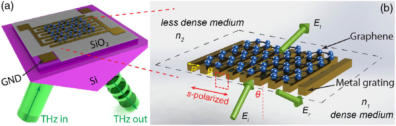
Fig. 2. (a) Simulation and calculation results of reflected intensity from a graphene/metal grating. The solid lines are calculation results, and the dots are simulation results with different enhancement factors (η x E η = 2

Fig. 3. Schematic of the experimental setup and photograph of the metal grating integrated graphene device. (a) Schematic of the graphene modulator in TIR geometry. (b) and (c) are photographs of the metal grating structure. (d) Photograph of the graphene area, showing clearly the graphene covered metal grating area and bare graphene area (white dashed outline).

Fig. 4. THz peak-to-peak images of two metal gratings without graphene in TIR geometry. The peak-to-peak values are calculated from the reflected THz electric field signal from the top surface of the devices. The direction of the electric field is represented by a red double-arrow line. The slit orientation of the grating is represented by golden lines. The white dashed outlines in the images highlight the grating areas. (a), (b) Images of the 30–15 μm grating with electric field perpendicular and parallel to the silt direction. (c), (d) Images of the 30–10 μm grating with electric field perpendicular and parallel to the slit direction.

Fig. 5. Experimental results of the metal grating integrated graphene device. (a), (b) THz peak-to-peak images of 30–15 μm and 30–10 μm grating devices without applying voltage. The graphene transferred on the metal grating is highlighted with white dashed lines. The right side of the graphene area is with a metal grating; the left side of the graphene area is without a covering metal grating. (c) and (d) are reflected waveforms by changing the gate voltages from − 60 V + 60 V

Fig. 6. (a) and (b) are MDs of the two devices in TIR and transmission geometries (T90). The red solid line is the MD of graphene integrated with a 30–10 μm grating; the blue solid line is the MD of graphene integrated with a 30–15 μm grating; the green dashed line is the MD of graphene without a metal grating.

Yiwen Sun, Riccardo Degl’Innocenti, David A. Ritchie, Harvey E. Beere, Long Xiao, Michael Ruggiero, J. Axel Zeitler, Rayko I. Stantchev, Danni Chen, Zhengchun Peng, Emma MacPherson, Xudong Liu. Graphene-loaded metal wire grating for deep and broadband THz modulation in total internal reflection geometry[J]. Photonics Research, 2018, 6(12): 12001151.


 PDF全文
PDF全文

