光学学报, 2018, 38 (1): 0111004, 网络出版: 2018-08-31
基于双色LED芯片的双波长像面数字全息显微术  下载: 1053次
Dual-Wavelength Image-Plane Digital Holographic Microscopy Based on Bi-Color LED Chips
图 & 表
图 1. 双色LED芯片的封装结构图。 (a)正视图;(b)俯视图;(c)电路图;(d)实物图
Fig. 1. Packaging structure of bi-color LED chips. (a) Front view; (b) top view; (c) circuit; (d) physical map
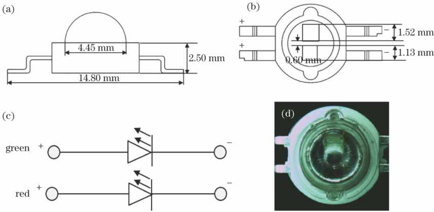


图 4. 彩色数字全息图。 (a)相移前;(b)相移后
Fig. 4. Colorful digital holograms. (a) Without phase shift; (b) with phase shift

图 5. 两种波长的相移数字全息图。(a) 670 nm波长相移前;(b) 670 nm波长相移后;(c) 521 nm波长相移前;(d) 521 nm波长相移后
Fig. 5. Phase shifting digital holograms with two wavelengths. (a) Without phase shift at 670 nm; (b) with phase shift at 670 nm; (c) without phase shift at 521 nm; (d) with phase shift at 521 nm

图 6. 通过两步相移算法重构的包裹相位图。 (a) 670 nm; (b) 521 nm
Fig. 6. Reconstructed wrap phase maps using two-step phase shifting algorithm. (a) 670 nm; (b) 521 nm

图 7. 实验结果。 (a)含有相位畸变的双波长合成相位;(b)去除相位畸变的双波长合成相位;(c)被测样品的三维面型分布;(d)对比实验结果
Fig. 7. Experimental results. (a) Dual-wavelength phase map with phase distortion; (b) dual wavelength phase map without phase distortion; (c) 3D surface profile of the tested sample; (d) comparison of the measurement data


表 1封装后双色LED芯片的光学性质
Table1. Optical properties of the utilized bi-color LED chips
|
邓丽军, 黄星艳, 曾吕明, 黄振, 刘国栋. 基于双色LED芯片的双波长像面数字全息显微术[J]. 光学学报, 2018, 38(1): 0111004. Lijun Deng, Xingyan Huang, Lüming Zeng, Zhen Huang, Guodong Liu. Dual-Wavelength Image-Plane Digital Holographic Microscopy Based on Bi-Color LED Chips[J]. Acta Optica Sinica, 2018, 38(1): 0111004.


 PDF全文
PDF全文

