Progress on waveguide-based holographic video (Invited Paper)  Download: 847次
Scanned aperture technology was first introduced as a solution for holographic video by the Spatial Imaging Group at the Massachusetts Institute of Technology (MIT)[1]. The MIT architecture uses an acousto-optic modulator (AOM) to create holographic patterns made of acoustic waveforms. As shown in Fig.
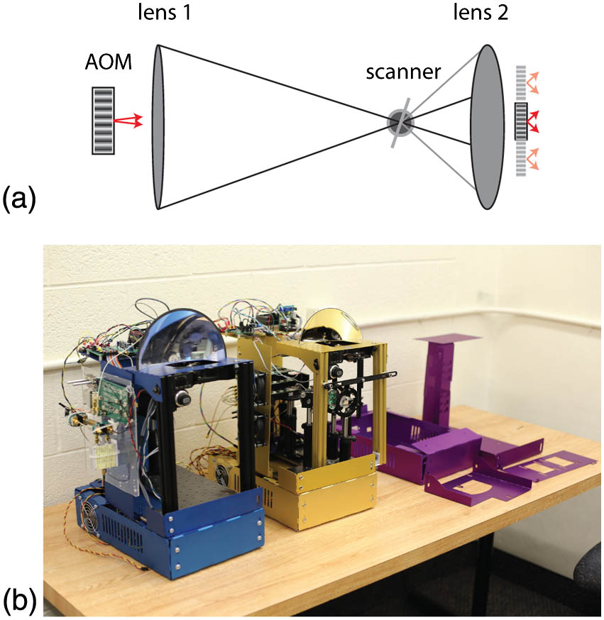
Fig. 1. (a) Scanned aperture holographic video architecture. (b) Holographic video monitors under construction at Brigham Young University.
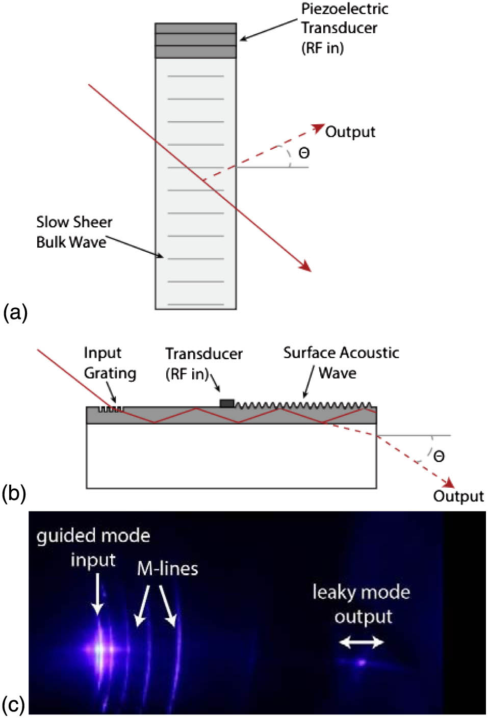
Fig. 2. (a) Bulk wave modulator. A slow sheer wave is emitted from the piezoelectric transducer, which interacts with the input light, deflecting it to
The supercomputer used to run the original prototypes was replaced by Bove
Smalley and colleagues also created a custom guided-wave modulator, fabricated on a lithium niobate substrate, to replace the tellurium dioxide Bragg cell [see Fig.
The guided to leaky-mode interaction provides a number of mechanisms for extracting noise from diffracted light. The guided to leaky-mode interaction can be used to convert transverse electric (TE) guided light into transverse magnetic (TM) polarized leaky-mode light. A polarizer can then be used to separate diffracted light from all other light in the system. Furthermore, the leaky-mode light escapes the confines of the waveguide and is angularly separated from the undiffracted or zero-order light, which remains trapped in the waveguide [see Fig.
The near-collinear illumination of the SAW pattern in the waveguide results in a much larger diffraction angle than is possible at near-normal incidence. This is a result of the nonlinear nature of the grating equation
Multichannel guide to leaky-mode modulators have other advantages over tellurium dioxide with respect to holographic video display. Tellurium dioxide, slow shear mode, Bragg cell AOMs can produce efficient, high-angle deflection thanks to their low acoustic wave speed and good acousto-optic properties, but they suffer from high acoustic attenuation when compared to lithium niobate, which prevents them from operating effectively beyond 100 MHz[9,10]. Lithium niobate has a much lower acoustic attenuation, which allows for the practical use of acoustic frequencies beyond 1 GHz and makes large acoustic bandwidths possible[11,12]. If using SAWs, lithium niobate may also produce lower-cost modulators than tellurium dioxide, in part because tellurium dioxide Bragg cells do not lend themselves to standard wafer-based fabrication processes.
The transducers that produce SAWs can be formed by standard photolithographic processes. The fabrication of these devices is described in Ref. [7].
The author and his colleagues have created an apparatus for the semi-automatic characterization of guided-wave devices[13]. This apparatus operates as shown in Fig.
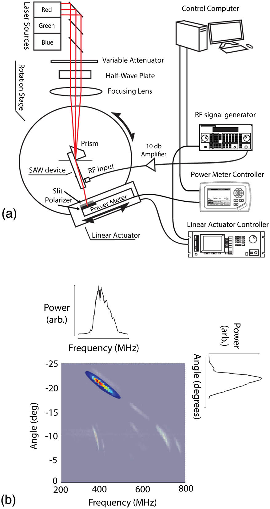
Fig. 3. (a) Semi-automatic characterization apparatus. For each step of the power meter the RF input frequency is swept and the resulting graph formed by this data is referred to in this paper as a “data map”. (b) Example of a data map. Note that the data map shows the optical output power of the guided-wave device as a function of both RF drive frequency and output angle. The
The reader will note that the data map contains several “islands” of optical output power. These islands correspond to specific guided to leaky-mode transitions in the device. Light entering the device travels in a discrete waveguide mode. Later, when it interacts with the SAW, this guided-mode light is converted to leaky-mode light. Each of these islands represents one of these guided to leaky-mode transitions.
These transitions can be modified by changing the waveguide parameters, such as the depth and index gradient profile. These changes affect the supported modes for a given wavelength of light in the waveguide. Light confined to a given mode has a certain momentum, represented by its wavenumber. Likewise, the SAW interacting with the light also has momentum. These momentums undergo vector addition, resulting in a loss of forward horizontal momentum in the mode of light. As a result, the mode is no longer confined to the waveguide and leaks out into the bulk substrate.
The angle of the propagation of the leaky-mode output light is directly related to the momentum of the SAW. By varying the frequency of the SAW the output light can be scanned or shaped. This leaky-mode output has both an RF and angular bandwidth that appears as an island on the data map.
By characterizing a number of samples using this apparatus, the authors were able to identify a device with a shallow waveguide capable of the frequency control of color[14]. For this device, the acoustic frequency response of red, green, and blue light is separated, but the output of these colors can be made to overlap. This makes it possible to modulate red, green, and blue light in a holographic display simply by changing the frequency content of the input signal, obviating the need for a color filter wheel or dedicated red, green, and blue channels.
Further testing showed that the bandwidth and center of the output frequency response could be manipulated by adjusting the waveguide parameters, such as depth, profile, and index of refraction (see Figs.
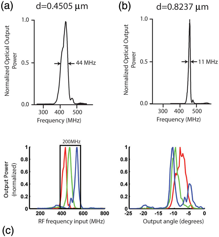
Fig. 4. (a) Frequency response for a guided-wave device with a shallow waveguide, (b) frequency response for a guided-wave device with a deep waveguide, and (c) frequency and angular response of a guided-wave device optimized for the frequency control of color.
The characterization apparatus is now being used to study other optimization criteria of interest, including linearity and slope. Data maps like the one shown in Fig.
![(a) Data map showing both nonlinear and linear outputs. (b) An image showing the composite output of a nonlinear transition as the RF input is swept from low frequency to high frequency in 6 MHz steps [an example of this type of transition is shown in the right part of (a)]. If the transition were linear, these spots would be separated uniformly. However, this transition is nonlinear, so we see a variation in deflection angle at high frequencies even though the frequency step is constant. (c) A data map showing output with both low and high slopes. Note that the both outputs cover a similar range of angles, but in the case of the high slope output this range is controlled by a much smaller RF bandwidth. One can chose the high or low slope transition, as desired, by modifying the launch conditions (input angle) of the illumination light at the input.](/richHtml/col/2016/14/1/010003/img_005.jpg)
Fig. 5. (a) Data map showing both nonlinear and linear outputs. (b) An image showing the composite output of a nonlinear transition as the RF input is swept from low frequency to high frequency in 6 MHz steps [an example of this type of transition is shown in the right part of (a)]. If the transition were linear, these spots would be separated uniformly. However, this transition is nonlinear, so we see a variation in deflection angle at high frequencies even though the frequency step is constant. (c) A data map showing output with both low and high slopes. Note that the both outputs cover a similar range of angles, but in the case of the high slope output this range is controlled by a much smaller RF bandwidth. One can chose the high or low slope transition, as desired, by modifying the launch conditions (input angle) of the illumination light at the input.
The characterization of guided-wave devices has made it possible to begin optimizing these devices for low-cost holographic video display. Using a custom-built characterization device, the authors have optimized the frequency control of color and bandwidth. They have used data maps to match aggregate device bandwidth to that of common GPU signals. The authors have identified transitions with both nonlinear and linear responses and are examining transitions with the potential for large angular deflections controlled by relatively small RF bandwidths.
As part of a future work, guided-wave devices may be optimized for other criteria important to holographic display, such as diffraction efficiency and point spread function. Data maps, such as those shown above, will continue to be important as these criteria are evaluated.
Future work will also include improving the function of input coupling gratings and exploring alternative device fabrication processes with the goal of increasing process throughput and yield. Now that optimal transducer parameters have been identified for RGB operation, it is desirable to eliminate the direct write step in the fabrication of transducers for guided-wave devices. The minimum feature size for the transducers is over 1 μm and it should be possible to pattern these transducers by photolithography. Such a process would involve first photolithographically patterning aluminum transducers, then covering the wafer and transducers with silicon nitride or silicon dioxide, and then patterning and proton exchanging waveguides. After the oxide or nitride is stripped, an intact wafer of devices should remain. Such a process would greatly increase device throughput. Also, using an expensive rutile prism to couple light into the guided-wave devices defeats the purpose of having created low-cost light modulators. The prisms could be replaced by grating input couplers.
It would be desirable to investigate how to best reduce cross talk between guided-wave channels to allow for the tightest possible channel packing in the light modulation devices. The authors would also like to investigate the effect of other proton exchange techniques on the quality of guided-wave devices.
Finally, new graphics cards are rapidly moving away from fast analog outputs toward greater numbers of digital outputs. It soon will be necessary to identify a driving scheme that can convert these digital signals to an analog holographic signal at low cost.
With each new optimization, guided-wave devices become better adapted to the challenges of scanned aperture holographic video. The work to date continues to suggest that these modulators have the potential to greatly broaden participation in holographic video by making available a low-cost approach to electroholographic display.
[1]
[2]
[3]
[4]
[5]
[6]
[7]
[8]
[9]
[11]
[12]
[13]
[14]
S. McLaughlin, C. Leach, S. Gneiting, V. M. Bove, S. Jolly, D. E. Smalley. Progress on waveguide-based holographic video (Invited Paper)[J]. Chinese Optics Letters, 2016, 14(1): 010003.
