1. INTRODUCTION
Depletion-type silicon ring modulators (Si RMs) attract a great amount of research interests since they can provide advantages for optical interconnect (IC) applications such as large modulation bandwidth and small power consumption [1–4" target="_self" style="display: inline;">–4]. Furthermore, Si RMs are much smaller than the widely used Si Mach–Zehnder modulators (MZMs) and, consequently, allow much easier monolithic integration with electronics. Such electronic–photonic integration is necessary for interconnection solutions for future high-performance electronic systems in which photonic solutions must be as closely located to electronics as possible for size and power consumption reduction [5]. To realize Si electronic–photonic ICs containing Si RMs, a Si RM equivalent circuit model that is accurate, easy-to-use, and compatible with the standard IC design environment is highly desirable. In addition, extracting numerical values for model parameters should be simple and straight-forward.
Although there have been several published reports on depletion-type Si RM models, none satisfies the above requirements. In Ref. [6], a precise analytical model for a Si RM was reported, but it requires more than 10 parameters and is not very compatible with the standard Si IC design environment. We reported a Verilog-A implementation of a coupled-mode description of the Si RM [7], which can be easily executed in the SPICE simulation environment. It, however, requires a substantial amount of computation time because Verilog-A is not optimized for numerically solving differential equations and, consequently, the simulation must use a very fine time resolution to accurately describe Si RM dynamics.
In this paper, we present a large-signal equivalent circuit model based on the linear equivalent circuit of the Si RM [8], which contains only a few independent model parameters that can be easily extracted from the simple RM transmission measurement. Although model parameter values nonlinearly depend on the Si RM bias voltage, we demonstrate that, by using voltage-dependent circuit elements available within SPICE, large-signal transient modulation characteristics can be easily and accurately simulated at least 220 times faster than the approach used in Ref. [7]. Such a reduction in computation time should provide a great advantage for design optimization of optical interconnection solutions for high-performance electronic systems that may contain numerous Si RMs as well as various electronic circuit blocks. An initial portion of this work was reported in Ref. [9]. In this paper, a more detailed description of our model is presented. In addition, we provide how our model can be used for performance optimization of pulse-amplitude modulation 4 (PAM-4) transmitters containing Si RMs and SiGe BiCMOS transistors.
This paper is organized in four chapters. In Chapter 2, after a brief description of the Si RM device used for our investigation, we give the details of our model and explain how model parameters are extracted from measurement results. The accuracy of the model also is verified with a 25 Gb/s non-return-to-zero (NRZ) measurement. In Chapter 3, we demonstrate the advantage of our model by showing how it can be used for the design optimization of a monolithic Si photonic NRZ and PAM-4 transmitters in terms of power consumption minimization and optical modulation amplitude (OMA) maximization. Chapter 4 concludes the paper.
2. LARGE-SIGNAL SPICE MODEL FOR Si RM
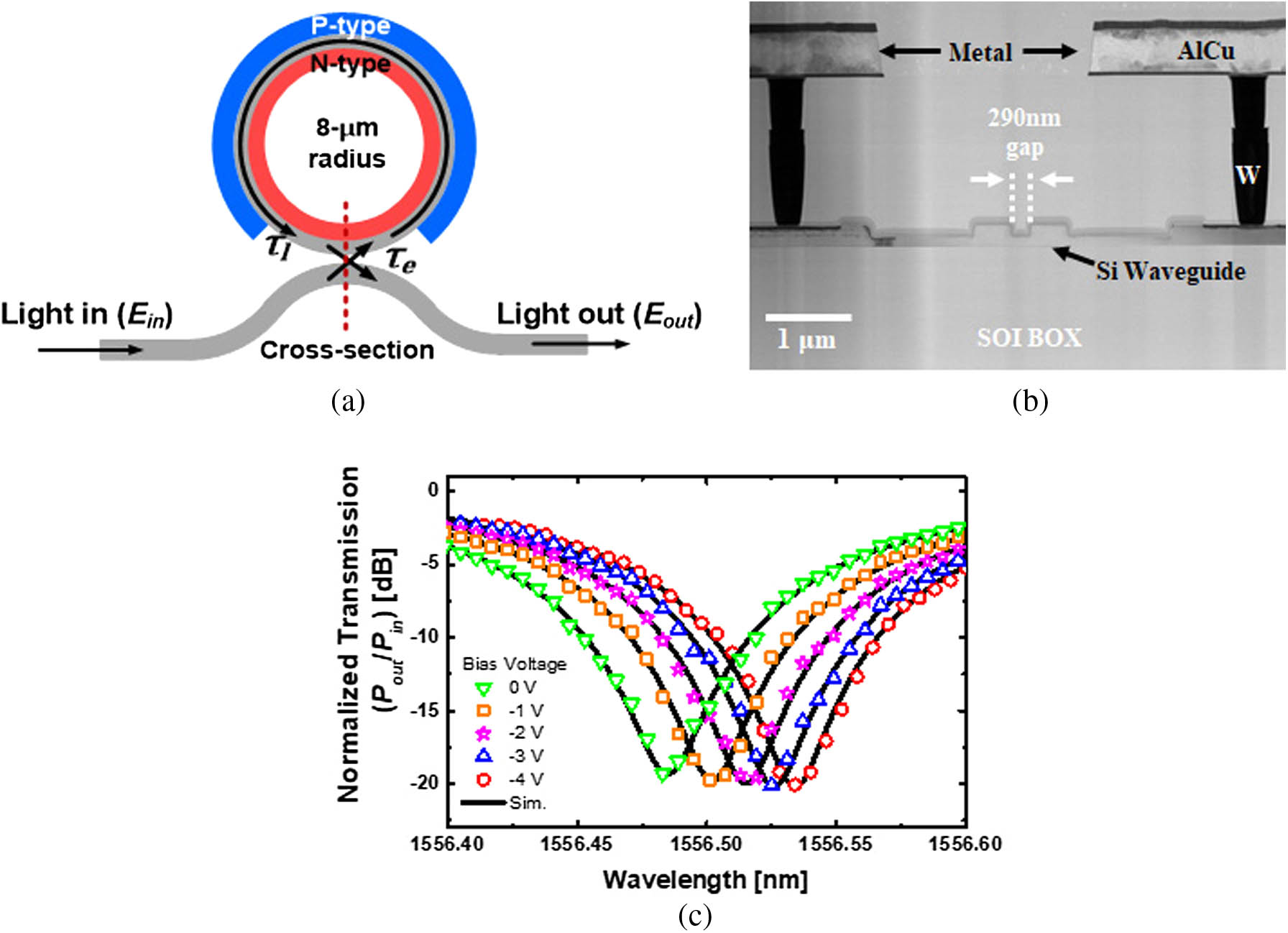
Figure 1(a) shows the structure of the depletion-type Si RM used for our investigation. It is fabricated by a Si photonics foundry service provided by IHP. The ring has an 8 μm radius, and there is a 290 nm separation between the bus and ring waveguides, as can be seen in the TEM image of the cross-section of the coupling section given in Fig. 1(b). The lateral p-n junction diode for the ring waveguide has the nominal peak doping concentration of for the p-region and for the n-region. Figure 1(c) shows the normalized transmission characteristics measured at four different bias voltages. For this and other measurements reported in this paper, the device is placed on a stage whose temperature is maintained at 25°C by a temperature controller.
Fig. 1. (a) Structure of the Si RM used; (b) TEM image of the cross-section of the coupling section; and (c) measured transmission curves with different bias voltages.
下载图片 查看所有图片
The dynamic characteristics of an RM can be described by coupled-mode equations as [10] where ) represents the energy stored in the ring resonator, and is the decay time constant for . has two components, and , which, respectively, represent the decay time constants due to the ring resonator loss and the coupling loss between the ring and bus waveguides. Their relationship is given as . is the ring resonance angular frequency given as , where is an integer representing the resonance mode index, is the velocity of light in the vacuum, is the ring circumference, and is the effective index of the ring waveguide at the resonance.
The RM steady-state transmission characteristics can be derived from Eqs. (1) and (2) as By fitting Eq. (3) to the measured transmission characteristics shown in Fig. 1(c), numerical values for three key parameters (, , ) at different bias voltages can be determined. The results are given in Table 1. The quality factor of the RM is related to as , which indicates our RM has a of about 8000.
Table 1. Extracted Si RM Parameters at Different Bias Voltages
| (V) | | (ps/rad) | (ps/rad) | | 0 | 2.632166 | 22.7239 | 12.8595 | | −1 | 2.632185 | 22.9560 | 12.9335 | | −2 | 2.632216 | 23.5576 | 13.1224 | | −3 | 2.632233 | 23.5578 | 13.1225 | | −4 | 2.632250 | 23.5579 | 13.1225 |
|
查看所有表
The normalized RM small-signal modulation frequency response in the -domain at a given bias voltage can be approximated as [11] where is the detuning parameter () representing how much the input light frequency () is separated from the RM resonance frequency (). Figure 2(a) shows the block diagram of the Si RM equivalent circuit. It consists of three blocks. Block A accounts for parasitic RLC components due to bond pads and metal interconnects [8]. Block B shown in Fig. 2(b) represents the RM’s electrical property due to a series resistance and ring waveguide p-n junction. Block C shown in Fig. 2(c) is an equivalent circuit emulating Eq. (4). Voltage-dependent resistors and capacitors are used in Blocks B and C, as the junction capacitance, and and depend on RM bias voltages. A scaling factor given as is used in Block C, where and are the input and output optical power used for the RM transmission measurement, respectively, so that Block C output voltage, , represents the ratio of and .
Fig. 2. (a) Three blocks for the Si RM model; (b) circuit representing RM electrical property; and (c) equivalent circuit representing RM optical property.
下载图片 查看所有图片
Numerical values for circuit elements in Blocks A and B can be easily obtained from the electrical -parameter measurements at different bias voltages. Numerical values for Block C circuit elements are obtained by matching Eq. (4) with the Block C transfer function given as using extracted numerical values for , , and at different bias voltages and detuning values. Table 2 shows the extracted numerical values for Block C circuit elements for two different cases of detuning wavelengths. The circuit models given in Block B and Block C are small signal models whose parameter values depend on bias voltages. With parameter values determined at a few sample bias voltages, large-signal behavior modeling can be easily done using the piece-wise linear simulation capability available in SPICE. Here, the detuning wavelength given as is used because it is more convenient to use in measurement. As can be seen in the table, is independent of the bias voltage and detuning, and is independent of detuning. Since Eq. (4) has three independent variables () and Eq. (5) has four (), we arbitrarily fix the value of at a 0 bias voltage as 10,000 Ω and then determine other circuit parameter values at the same bias voltages. For other bias voltages, we fix the value of at the value determined at 0 bias voltage and modify other resistor and capacitor values since variable resistors and capacitors are much easier to use in SPICE than the variable inductor. does not change with since does not depend on . On the other hand, is proportional to , and is proportional to , which does not depend on . Consequently, decreases with .
Table 2. Values for Si RM Equivalent Circuit Model Parameters for the Case of and 70 pm
| (V) | () | (fF) | () | (fF) | () | (nH) | | and 70 pm | | | | | and 70 pm | and 70 pm | | 0 | 249 | 14.26 | 0.35 | 2.07 | 42.15 | 7.14 | 10.00 | 114.41 | | −1 | 10.95 | 0.75 | 3.15 | 19.65 | 4.70 | 9.96 | | −2 | 9.47 | 1.77 | 5.15 | 8.37 | 2.87 | 9.71 | | −3 | 8.55 | 3.01 | 7.19 | 4.92 | 2.06 | 9.71 | | −4 | 7.90 | 4.20 | 8.99 | 3.52 | 1.65 | 9.71 |
|
查看所有表
The voltage-dependent circuit elements in Fig. 2(b) can be easily implemented with the piece-wise linear (PWL) elements available in SPICE. Using this approach, the large-signal RM eye diagrams can be very easily simulated in SPICE. Although parameter values at only five different biases are specified for our investigation, the simulator automatically interpolates the values at other bias voltages, providing very accurate and efficient simulation results. Figure 3 shows both the measured and simulated (red lines) 25 Gb/s Si RM eye diagrams for several detuning values. For both, modulating signals are PRBS having with common mode voltage. For simulation, Synopsys HSPICE, Version M 2017.03, is used. In addition, S21 responses of RF cables, the oscilloscope (Tektronix CSA8000B and 80E03), and the optical receiver (Optilab PR-23-M) [12] used in the measurement are included to achieve an accurate comparison. As can be seen, the simulation based on the RM equivalent circuit provides good agreement with the measurement results. For a 1 μs long transient simulation with a 0.1 ps time step, the approach reported in Ref. [7] requires 980 s in computation with two octa-core Intel processors (E5-2640 v3) and 32 GB RAM, whereas our new approach needs only 4.43 s in the same computation environment, providing performance that is 220 times faster. As can be seen in Fig. 3, data with as 70 pm shows the largest OMA.
Fig. 3. Measured and simulated (red line) 25 Gb/s PRBS31 eye diagrams for different .
下载图片 查看所有图片
3. CO-SIMULATION OF Si RM AND SiGe BiCMOS DRIVER
The real advantage of our model is the ease with which it can be used for co-simulation of electronic circuits and Si RMs. Figure 4(a) shows a schematic diagram for an integrated 25 Gb/s Si photonic transmitter containing a fully differential cascode common-emitter driver and a Si RM. The driver employs the source degeneration technique with to enhance the transmitter bandwidth. This kind of electronic–photonic integrated circuits can be monolithically fabricated with IHP’s photonic BiCMOS technology, which provides high-performance SiGe bipolar transistors having of 220/290-GHz and Si photonic components on the same Si platform [13]. With our RM circuit model, the design optimization of the entire transmitter can be easily carried out.
Fig. 4. (a) Schematic diagram for an integrated 25 Gb/s Si photonic transmitter based on Photonic BiCMOS technology; (b) vertical eye opening for various and values; and (c) simulated eye diagrams at different and combinations.
下载图片 查看所有图片
Figure 4(b) shows the simulated vertical eye opening normalized to the input optical power at different values of and for the case of to have the largest OMA. and are key parameters in the driver that determine eye opening, power consumption, and bandwidth. For the simulation, 25 Gb/s PRBS NRZ data with a 600 mV swing are supplied to and . Also, the power supply of the driver circuit () was 4.5 V to have the output data of the driver circuit as . Post-layout parasitic RC values for the driver are included in the simulation since they can significantly influence the driver performance. As can be seen in Fig. 4(b), the vertical eye opening strongly depends on and values. The optimal condition can be determined that provides the largest modulator output eye opening with the smallest , or the smallest power consumption. With a fixed value for , larger generates a larger output voltage swing but runs into the headroom problem if is too large. Figure 4(c) shows simulated eye diagrams at three different conditions, whose and values are represented by Points A, B, and C in Fig. 4(b), having at the driver output. Point A requires a small for peak eye opening but experiences degradation due to a large RC time constant, as shown in the simulated eye diagram. Points B and C show similar eye patterns in terms of rising and falling times but Point C requires a larger due to a smaller , which results in a larger power consumption. Consequently, Point B provides the largest eye opening with the smallest power consumption.
Our RM circuit model can also be used to optimize the ratio of level mismatch (RLM), which is the key performance parameter for a PAM-4 transmitter. RLM is defined as where , , and are defined in Fig. 5. PAM-4 allows a higher data rate transmission without requiring a higher transmitter bandwidth, and it is the standard for many important high-speed I/O applications [14,15]. There is growing interest in PAM-4 based on Si RMs [16–20" target="_self" style="display: inline;">–20], but its performance is greatly affected by Si RM nonlinearity, which results in degraded RLM [16–20" target="_self" style="display: inline;">–20]. This nonlinearity is due to the Lorentzian shape of the RM resonance as well as the nonlinear dependence of the ring waveguide effective index on the reverse bias [20]. This poses a great challenge to achieve Si PAM-4 transmitters because there is a rather tight requirement on RLM. RLM higher than 94%, for example, is required for IEEE802.3bs and CEI-56G [14,15]. One solution is to apply different driving voltages for , , and , which can compensate for RM nonlinearity [20,21]. To use this approach, an accurate co-simulation of a driver circuit and RM is essential.
Fig. 5. PAM-4 eye diagram and level representation.
下载图片 查看所有图片
Figure 6(a) shows a schematic diagram for an integrated 25 GBaud PAM-4 Si photonic transmitter containing a Si RM and a fully differential cascode BiCMOS common-emitter driver with the emitter degeneration based on IHP photonic BiCMOS technology. To determine the optimum PAM-4 modulation condition, SPICE simulation is performed for the integrated transmitter for varying RM values and different RLM values for the driver output voltages measured between (). For the simulation, is selected based on the optimization carried out for the above-mentioned NRZ transmitter. Data (25 Gb/s PRBS NRZ) is supplied to both inputs of MSB and LSB ports.
Fig. 6. (a) Schematic diagram of the PAM-4 Si photonic transmitter including driver circuit and the RM and (b) simulated values for various combinations of and values.
下载图片 查看所有图片
The entire transmitter, including the driver and the Si RM, is simulated using the equivalent circuit for Si RM. Figure 6(b) shows the resulting RLM for the Si RM output, or for varying driver output voltage RLM, or , and detuning. Different values are achieved by changing and , while their sum is kept the same and has a swing. As can be seen in the figure, over 94% can be achieved when is about 80 pm and the is between about 75% and 85%. Figure 7 shows the simulated eye diagrams for the driver and RM outputs in different conditions represented by Points A, B, C, and D in Fig. 6(b), and such conditions and results are described in Table 3. At Point A, is almost 100% but is significantly degraded due to Si RM nonlinearity. The RM nonlinearity is such that the middle eye opening is the largest. Consequently, by distorting driver output or making the middle eye smaller, can be improved, as shown by the Points B and C eye diagrams. Too much driver output distortion causes degradation, as shown by the Point D eye diagram. With the optimum distortion of the driver output, we can carefully choose the detuning for the maximum , as Point C shows an almost 97% RLM value.
Fig. 7. Simulated 25 GBaud PAM-4 eye diagrams at different combination of and .
下载图片 查看所有图片
Table 3. Operating Conditions and Simulated Results for Different Points in Fig. 6
| | | | | Point A | 97.8% | 80 pm | 75.5% | | Point B | 78.9% | 90 pm | 88.5% | | Point C | 78.9% | 80 pm | 96.9% | | Point D | 67.2% | 80 pm | 82.0% |
|
查看所有表
4. CONCLUSION
We demonstrate a new large-signal SPICE circuit model for a depletion-type Si RM. The model is accurate, easy to use, and allows a significantly reduced simulation time compared to the previously reported approach. The accuracy of the model is confirmed with measured 25 Gb/s NRZ modulation results at different detuning values. Furthermore, the model allows easy co-simulation with electronic driver circuits. We demonstrate the design optimization based on such co-simulation for Si NRZ and PAM-4 transmitters containing SiGe BiCMOS drivers and Si RMs.
5 Acknowledgment
Acknowledgment. We thank IC Design Education Center (IDEC) for EDA tool support.
Minkyu Kim, Myungjin Shin, Min-Hyeong Kim, Byung-Min Yu, Younghyun Kim, Yoojin Ban, Stefan Lischke, Christian Mai, Lars Zimmermann, Woo-Young Choi. Large-signal SPICE model for depletion-type silicon ring modulators[J]. Photonics Research, 2019, 7(9): 09000948.
 Download: 739次


