Chinese Optics Letters, 2020, 18 (9): 093201, Published Online: Jul. 24, 2020  

Regular uniform large-area subwavelength nanogratings fabricated by the interference of two femtosecond laser beams via cylindrical lens Download: 715次

Author Affiliations
1 State Key Laboratory of Precision Spectroscopy, School of Physics and Electronic Science, East China Normal University, Shanghai 200241, China
2 Collaborative Innovation Center of Extreme Optics, Shanxi University, Taiyuan 030006, China
Abstract
Inhomogeneity and low efficiency are two important factors that hinder the wide application of laser-induced periodic surface structures. Two-beam interference is commonly used to fabricate gratings with interference periods. This study reports regular and uniform periodic ripples fabricated efficiently by the interference of two femtosecond laser beams via a cylindrical lens. The interference period is adjusted to be an integer multiple of the wavelength of a surface plasmon polariton. Regular and uniform subwavelength nanogratings (RUSNGs) on a silicon wafer of a diameter of 100 mm are fabricated with a scanning velocity of 6–9 mm/s. Bright and pure colors (including purple, blue, and red) are demonstrated on different patterns covered with RUSNGs.

Laser-induced periodic surface structures have been extensively studied in various materials[15" target="_self" style="display: inline;">5], and exhibit a great potential for application in various areas such as structural coloring, birefringent optical elements, wettability, broadband absorption, and enhanced photoluminescence[612" target="_self" style="display: inline;">12]. Considerable effort has been devoted toward the production of regular periodic ripples using a femtosecond laser. Long-range uniform periodic structures were efficiently fabricated by femtosecond laser irradiation focused by a cylindrical lens[8,13]. Nevertheless, this technique faces many challenges in obtaining regular uniform nanostructures with high efficiency. The two main factors are that the ripple periods change significantly with laser fluence and scanning velocity[1417" target="_self" style="display: inline;">17]. During a sequence of laser pulses irradiation, the deposited debris and irregular microstructures induced by the preceding pulses cause the ripples to bend, split, and break[18,19].

Laser interference lithography has been widely applied to the fabrication of large-area micro/nanogratings[19,20]. To fabricate a grating with interference spacing less than the laser wavelength, the angle between two laser beams must be larger than 60°. For a femtosecond laser, the focus diameter is usually only tens of microns (μm), and this requires that the straightness of three translation stages should be less than 10 μm in total for excellent interference fringes. However, it is not economical to achieve this extremely high precision in the industry. In this study, we built a double cylindrical lens interference setup with a small angle of 9.3° based on an 800 nm, 50 fs, 3.5 mJ, and 1 kHz laser system (Legend Elite, Coherent). The interference spacing is 4.94 μm, seven times the wavelength of a surface plasmon polariton (SPP). Interestingly, regular uniform nanogratings with a period of SPP wavelength, instead of the interference period, were fabricated at the scanning velocity of 69mm/s. In addition, the graphic pattern of “raining of petals” and two types of flowers with nanogratings in different directions are fabricated, where the silicon wafer is mounted on an x/y/z/θ four-axis translation stage. These flowers exhibit bright pure colors observed with a charge-coupled device (CCD) in different directions.

Figure 1 shows that the laser beam goes through a half-wave plate and Glan prism to change the laser power and the polarization in the horizontal direction. The mechanical shutter is used to control the laser irradiation time. The 800 nm femtosecond laser beam is split into two using a splitter of 50%:50%, of which one beam transits via a delay line and arrives at the sample surface at the same time as the other, where the zero point is determined by the frequency-doubled signal of a barium borate (BBO) crystal. The angle 2θ between the two laser beams is set as 9.3°, and the interference period Λ is calculated as 4.94 μm using the equation Λ=λ/2sinθ (laser wavelength λ=0.8μm). The laser focuses of the two cylindrical lenses are 50 μm wide and 10 mm long. The centers of the two cylindrical lenses and the laser focus are perfectly aligned, with an error within ±0.1mm. Further, the silicon wafer is mounted on an x/y/z/θ four-axis translation stage. When the sample moves by ±50mm in the x/y plane, the laser focus shifts in the z direction with an error within ±5μm, which is adjusted using a laser range finder (Hong Chuang Tec/PL-IG50) with an accuracy of ±1μm. The experimental setup and the accuracy of adjustment ensure a perfect coincidence and stable interference of the two laser beams and can be used to fabricate regular and uniform subwavelength nanogratings (RUSNGs) in a large area in any designed direction.
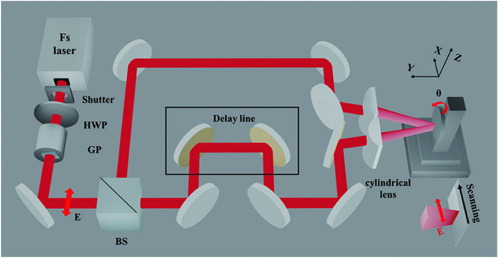
Fig. 1. The experimental setup of femtosecond laser interference via two cylindrical lenses. HWP is half-wave plate, GP is Glan prism, and BS is beam splitter. The double arrow E represents laser polarization.

下载图片 查看所有图片

The sample used in this study is a commercially available undoped Si wafer (100) of diameter 100 mm and thickness 0.5 mm. The surface is optically polished with a roughness of <1nm. Before laser processing, the silicon wafer was dipped in an acetone solution and sonicated for 5 min to remove the contaminating impurities and was then washed with pure water. After laser irradiation, the surface nanostructures were rinsed in hydrofluoric (HF) acid solution (5 mol/L) for 30 min to remove the oxidation and the ablation fragments before measuring with scanning electron microscopy (SEM)[17,21].

After single pulse radiation, only interference stripes of size 50 μm ×5.8mm are found in the ablation area. These interference stripes cause SPP excitation during the second laser pulse radiation and induce shallow subwavelength ripples that cover the interference stripes themselves. After three laser pulse radiations, very regularly spaced nanogratings of period 707±10nm are formed on the interference stripes, as shown in Fig. 2 (Visualization 1). The interference period Λ is measured as 4.94 μm, which agrees well with the theoretical value[6,10].
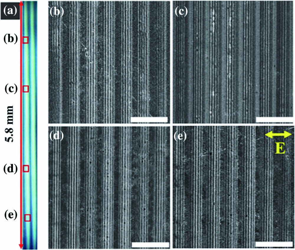
Fig. 2. Microstructures in the ablation area after radiation of three laser pulses. (b)–(e) Enlarged SEM pictures of the areas in squares in (a). The double arrow in (e) represents laser polarization. Laser fluence of single beam is 1.3J/cm2, and the scale bars are 5 μm.

下载图片 查看所有图片

The SPP excitation causes periodic distribution of the light field and further induces subwavelength periodic ripples; in addition, the SPP wavelength greatly varies with the dielectric constant in the excited state[2]. Because of the Gaussian distribution of the light field, the local dielectric constant, as well as the ripple period, at the center is much different from that at the edge of the ablation spot[16]. However, the SEM images in Figs. 2(b)2(e) illustrate that the ripple periods are mostly similar at about 707±10nm, although the ripple depth is different because of the light intensity.

During laser irradiation, a large amount of debris and surface defects are generated on the ablation spot, which greatly affects the SPP propagation, resulting in curved ripples with many breaks and bifurcations[18,19]. However, the nanogratings are very straight and continuous, despite the presence of some deposited particles. The ripple periods are mostly similar at about 707±10nm, which do not change greatly with local laser fluence. Moreover, the nanogratings are very straight and continuous, despite the presence of deposited particles. These phenomena are very interesting, but also much unexpected.

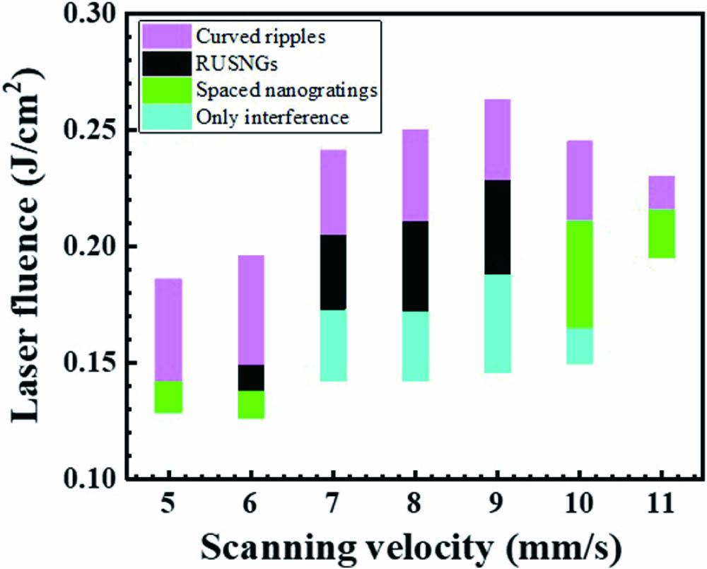
Subwavelength periodic ripples are effectively generated on the surface of silicon by direct writing with a single laser beam. Figure 3(a) shows that these ripples are curved with many breaks and particles. However, RUSNGs with a period of 707 nm cover the whole ablation area by two-beam interference [Fig. 3(b)]. Figure 3(c) shows that RUSNGs without etching in HF solution are covered with the oxidized particles and ablation fragments. The subwavelength ripples presented in Fig. 3(c) are much coarser than those in Fig. 3(b). The scanning velocity is 6.2 mm/s, and the laser fluence is 0.14J/cm2. Figure 4 illustrates different types of micro/nanostructures fabricated by changing the laser fluence and scanning velocities, where the laser frequency is constant at 1000 Hz. When the scanning velocity is in the range 6.09.0mm/s, and the laser fluence is in the range of 0.180.22J/cm2, the RUSNGs cover the entire ablation area. When the scanning velocity increases to 10–11 mm/s, spaced nanogratings are formed; when the laser fluence is 0.160.21J/cm2, and the scanning velocity is 5mm/s, no RUSNGs are formed on the sample surface.

Fig. 3. (a) Subwavelength periodic ripples by direct writing with a single laser beam. (b) RUSNGs ripples fabricated by direct writing of two-beam interference. (c) RUSNGs ripples without etching in HF solution. The double arrow E represents laser polarization, and the narrow ellipse represents the laser focus.
下载图片 查看所有图片

Fig. 4. Different types of micro/nanostructures depending on the laser fluence and scanning velocity.

下载图片 查看所有图片

Interestingly, the periods of all RUSNGs are similar (707±10nm), irrespective of any higher value of laser fluence and scanning velocity, as presented in Fig. 5. Similarly, the periods of all the spaced nanogratings are 707±10nm. These results are significantly different from those obtained for a single laser beam. When the scanning velocity decreases from 15 to 4 mm/s, the period of ripples induced by the single laser beam decreases from 788 to 664 nm.
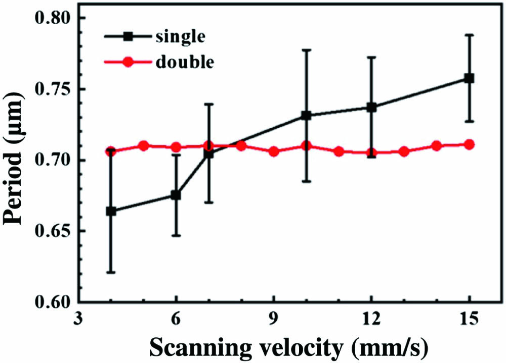
Fig. 5. Periods of subwavelength ripples as a function of scanning velocity induced by a single laser beam and two-beam interference.

下载图片 查看所有图片

The interference period Λ is 4.94 μm, seven times the SPP wavelengths. When the size of a microcavity is an integer multiple of surface plasmon wavelengths, the local field intensity enhances greatly for the resonance enhancement. We propose that the resonance-enhanced SPP imposes a strong constraint on the generation of periodic ripples and has an excellent anti-disturbance ability. The formation mechanism of RUSNGs should be studied in detail in the future (Supplementary Material 1).

The RUSNGs in a large area are fabricated by direct writing of two-beam interference by scanning the sample in a succession of lines[22,23]. Figure 6 shows the coloring surface and SEM image of nanogratings with a period of 707 nm. The laser fluence is 0.14J/cm2, scanning velocity is 6.2 mm/s, and the space between adjacent scanning lines is 0.5 mm. A silicon wafer of diameter 100 mm can be processed to obtain a colored surface in 40 min.
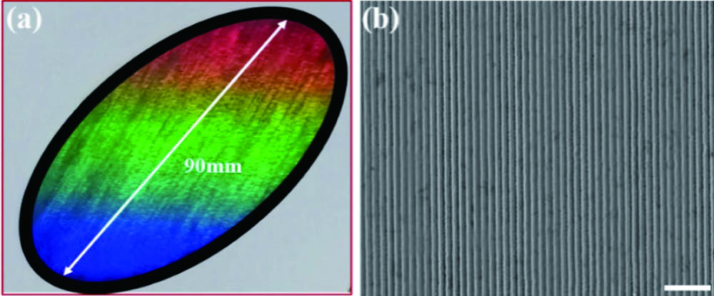
Fig. 6. (a) Optical image of the colored surface and (b) SEM image of RUSNGs. The scale bar is 5 μm.

下载图片 查看所有图片

To test the performance of the RUSNGs fabricated by this method, a wide-spectrum light source (4002200nm, tungsten halogen lamp) is perpendicularly illuminated on the sample surface, and the diffraction spectra are measured using a fiber spectrometer at different angles, as shown in Fig. 7(I). Furthermore, the full width at half-maximum (FWHM) data of different angles were collected, which served as a reference for the spectral ability of RUSNGs. For the reliability of plentiful statistical data, each diffraction spectrum was measured three times.
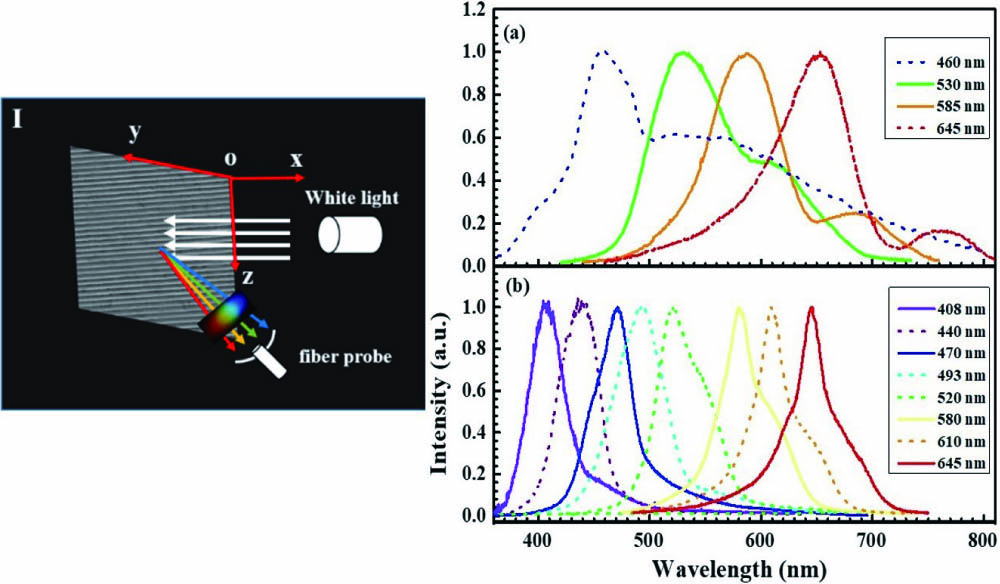
Fig. 7. Optical characterization measurements of the periodic ripples. (I) Diagrammatic sketch of the diffraction spectra test; diffraction spectra of (a) subwavelength ripples generated by single laser beam and (b) RUSNGs.

下载图片 查看所有图片

Two different samples, subwavelength ripples generated by scanning a single laser beam, and the RUSNGs fabricated by two-beam interference, are mounted at the same stage in sequence. The measured diffraction spectra are shown in Fig. 7. The diffraction peaks from the periodic ripples induced by a single laser beam are very wide, with an FWHM of 65140nm, as presented in Fig. 7(a). The diffraction efficiency of blue light is very low, and the near ultraviolet spectrum (<430nm) is invisible, because the periodic ripples are curved and contain many distortions and breaks. These defects increase the absorption of incident light and cause destructive interference. In addition to the low diffraction efficiency and wide peaks, even small impurity diffraction peaks are present, such as the orange and red spectra. Figure 7(b) shows that the diffraction peaks of RUSNGs are very narrow, especially those of blue and purple, with FWHM of only 3741nm. Compared with the subwavelength ripples induced by a single laser beam, the diffraction efficiency of RUSNGs is greatly improved. The intensities of blue, green, and red peaks are enhanced by 45, 16, and 28 times, respectively. Thus, the colored surface of the RUSNGs is very bright.

The Commission Internationale de l’Eclairage (CIE) xy chromaticity diagram is presented in Fig. 8, in which the colors found in the RUSNGs and subwavelength ripples induced by single laser beams are illustrated. The range of colors of RUSNGs is much wider than that of subwavelenth ripples. The CIE diagram indicates that the color saturation (i.e., Chroma) increases from the center and extends outward[24]. For an isochromatic wavelength line (λ=530nm), the coordinates are (0.28, 0.45), (0.28, 0.46), and (0.15, 0.81), and the color purity increases from 25.7% to 65.6% for the subwavelength ripples and the RUSNGs, respectively. For an isochromatic wavelength line (λ=475nm), the color purity is enhanced by 3.8 times and increases from 16.2% to 77.3%. The great increase in Chroma values of the blue, green, and red regions readily forms significantly vivid colors for the RUSNGs.
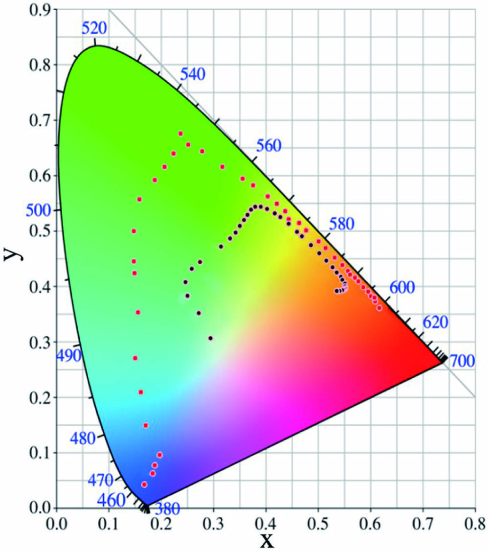
Fig. 8. CIE xy chromaticity diagram showing the colors of the RUSNGs (red dots) and subwavelength ripples (black dots).

下载图片 查看所有图片

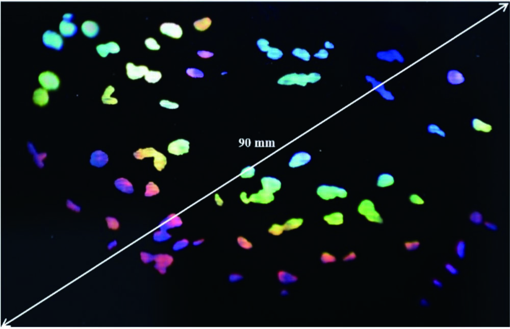
Different patterns in tin foil are fabricated by two-dimensional (2D) laser scanning and cover on the Si wafer. The RUSNGs are formed in patterns by direct writing of two-beam interference, which presents more excellent structural colors[6,25]. Figure 9 shows the colorful optical image of the pattern of “raining of petals” on a silicon wafer. The structure color, specifically blue and red, of the subwavelength ripples on silicon induced by a single laser beam is usually not sufficiently bright. However, all the petals of RUSNGs, including blue, red, and purple, are vivid.

Fig. 9. Colorful optical image of the pattern of “raining petals” covered with RUSNGs.

下载图片 查看所有图片

By adjusting the azimuth angle of the laser focus relative to the center of the rotatory stage and scanning the sample in the horizontal direction, nanogratings in different directions can be fabricated. A schematic of the processing method is shown in Fig. 10(I), where the red spikes represent laser spots, O denotes the center of the rotatory stage, two short green arrows on the circle represent the rotation direction, and the thick orange arrow represents the scanning direction. Figures 10(a) and 10(b) show the colorful optical images of two flowers with 10 petals. In each petal of flower A, the nanogratings are in the azimuth direction, whereas those on flower B are in the radial direction; thus, the colors of the two flowers differ greatly. Each petal of flower A is colorful, whereas that in flower B is bright and pure (Supplementary Material 2).
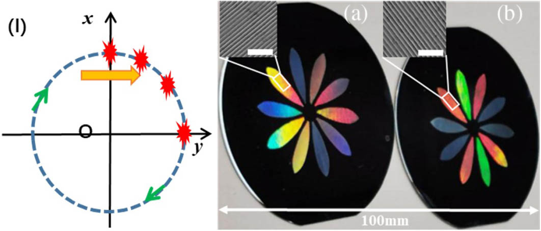
Fig. 10. Colorful optical images of two flowers with nanogratings in different directions. (I) Schematic of the processing method. Flowers with nanogratings in (a) azimuth direction and (b) radial direction. The two enlarged SEM pictures represent the nanogratings in the corresponding squares. The scale bars are 5 μm.

下载图片 查看所有图片

In conclusion, this study demonstrated an efficient method to fabricate RUSNGs by two-beam interference via two cylindrical lenses. The interference period was adjusted to be an integer multiple of the SPP wavelength, and RUSNGs with a period of 707±10nm were fabricated on a silicon wafer with the scanning velocity of 69mm/s. Complex cross-scale patterns with RUSNGs in different directions were fabricated when the wafer was mounted on an x/y/z/θ four-axis translation stage. These patterns exhibited vivid structural colors at different angles. The processing method proposed in this study presents potential applications in the fields of surface structural colors, birefringent optical elements, data storage, broadband absorption, and enhanced photoluminescence.

References

[1] SipeJ.YoungJ.PrestonJ.Van DrielH., Phys. Rev. B27, 1141 (1983).

[2] HuangM.ZhaoF.ChengY.XuN.XuZ., ACS Nano3, 4062 (2009).

[3] SunQ.LiangF.ValléeR.ChinS., Opt. Lett.33, 2713 (2008).OPLEDP0146-9592

[4] WangG.JiangL.SunJ.HuJ.WangQ.LiM., Chin. Opt. Lett.17, 081405 (2019).CJOEE31671-7694

[5] WuB.WangC.LuoZ.LiJ.ManS.DingK., Chin. Opt. Lett.18, 013101 (2020).CJOEE31671-7694

[6] WuH.JiaoY.ZhangC.ChenC.YangL.LiJ.NiJ.ZhangY.LiC.ZhangY.JiangS.ZhuS.HuY.WuD.ChuJ., Nanoscale11, 4803 (2019).NANOHL2040-3364

[7] BaoZ.WangC.ZhangY.ZhaoQ., Photon. Res.3, 180 (2015).

[8] WangL.ChenQ.CaoX.BuividasR.WangX.JuodkazisS.SunH., Light Sci. Appl.6, e17112 (2017).

[9] YangY.YangJ.LiangC.WangH., Opt. Express16, 11259 (2008).OPEXFF1094-4087

[10] JiaX.JiaT.ZhangY.XiongP.FengD.SunZ.XuZ., Opt. Express18, 14401 (2010).OPEXFF1094-4087

[11] XiongP.JiaT.JiaX.FengD.ZhangS.DingL.SunZ.QiuJ.XuZ., New J. Phys.13, 023044 (2011).NJOPFM1367-2630

[12] QiaoH.YangJ.WangF.YangY.SunJ., Opt. Express23, 26617 (2015).OPEXFF1094-4087

[13] HuangJ.JiangL.LiX.WeiQ.WangZ.LiB.QuL., Adv. Opt. Mater.7, 1900706 (2019).2195-1071

[14] MiyajiG.MiyazakiK., Appl. Phys. Lett.103, 071910 (2013).APPLAB0003-6951

[15] PanA.SiJ.ChenT.LiC.HouX., Appl. Surf. Sci.368, 443 (2016).ASUSEE0169-4332

[16] HuangM.XuZ., Laser Photon. Rev.8, 633 (2014).

[17] WangL.XuB.CaoX.LiQ.TianW.ChenQ.JuodkazisS.SunH., Optica4, 637 (2017).

[18] YangM.WuQ.ChenZ.ZhangB.TangB.YaoJ.Drevensek-OlenikI.XuJ., Opt. Lett.39, 343 (2014).OPLEDP0146-9592

[19] MurphyR.TorralvaB.AdamsD.YalisoveS., Appl. Phys. Lett.102, 211101 (2013).APPLAB0003-6951

[20] GuayJ.Calà LesinaA.BaxterJ.KillaireG.RamunnoL.BeriniP.WeckA., Adv. Opt. Mater.6, 1800189 (2018).2195-1071

[21] WillekeG.KellermannK., Semicond. Sci. Technol.11, 415 (1996).SSTEET0268-1242

[22] FuentesY.GarciaM.PuertoD.FlorianC.GarciaA.SanchezS., Sci. Rep.7, 4594 (2017).SRCEC32045-2322

[23] Hong RusliL.WangX. C.ZhengH. Y.WangH.YuH. Y., Appl. Surf. Sci.297, 134 (2014).ASUSEE0169-4332

[24] GuayJ.Calà LesinaA.CôtéG.CharronM.PoitrasD.RamunnoL.BeriniP.WeckA., Nat. Commun.8, 16095 (2017).NCAOBW2041-1723

[25] JiangH.ZhangY.HanD.XiaH.FengJ.ChenQ.HongZ.SunH., Adv. Funct. Mater.24, 4595 (2014).AFMDC61616-301X

Kaiqiang Cao, Long Chen, Ke Cheng, Zhenrong Sun, Tianqing Jia. Regular uniform large-area subwavelength nanogratings fabricated by the interference of two femtosecond laser beams via cylindrical lens[J]. Chinese Optics Letters, 2020, 18(9): 093201.

引用该论文: TXT   |   EndNote

相关论文

加载中...

关于本站 Cookie 的使用提示

中国光学期刊网使用基于 cookie 的技术来更好地为您提供各项服务,点击此处了解我们的隐私策略。 如您需继续使用本网站,请您授权我们使用本地 cookie 来保存部分信息。
全站搜索
您最值得信赖的光电行业旗舰网络服务平台!