激光与光电子学进展, 2019, 56 (23): 230001, 网络出版: 2019-11-27
自组装胶体晶体在微纳光学领域的研究进展  下载: 2019次封面文章
Self-Assembled Colloidal Crystals in Field of Micro-Nano Optics
图 & 表
图 1. 改变结构色或光子带隙的工艺。(a)圆盘结构和圆环结构的制备过程[33];(b1) PS纳米球在PDMS涂层上摩擦后的扫描电镜照片像[34];(b2)不同倾斜角度(θ )、方位角(Q )、距离下的不同颜色[34];(c) ABABAB堆积型光子晶体超晶格制备流程[35]
Fig. 1. Fabrication process for changing structural color or photonic band gap. (a) Schematic of fabrication processes of disk and ring structures[33]; (b1) scanning electron microscope (SEM) images of PS nanosphere after rubbing on PDMS-coated glass slide[34]; (b2) different colors depended on tilted angle (θ ), azimuthal angle (Q ), and sample-to-eye distance[
图 2. 彩色打印的相关工艺。(a1)喷墨打印法示意图[36];(a2)入射角60°下的衍射光谱[36];(a3)不同入射角度下不同波长光的反射率[36];(b)“滴铸法”示意图[37];(c)喷银打印示意图[38];(d)蒙德里安画作的厘米级临摹图像[39]
Fig. 2. Fabrication processes related to color printing. (a1) Schematic of printing process using inkjet printer[36]; (a2) diffraction spectra with incident angle θ i=60°[36]; (a3) reflectivity of light with different wavelengths at different incident angles[36]; (b) schematic of “drop-casting” procedure[
图 3. 彩色打印的相关工艺。(a)光子晶体薄膜的夹层结构制备示意图[40];(b)自组装ACAs示意图[41];(c)在相纸基底上打印CdS图案工艺的示意图[42];(d1)(d2)制备胶体晶体图案的工艺流程[43];(d3)反射光谱及其光学显微照片[43]
Fig. 3. Fabrications related to color printing. (a) Schematic of fabrication process of sandwich structure using freestanding photonic crystal film[40]; (b) schematic of self-assembled ACAs[41]; (c) schematic of inkjet printing process of CdS pattern on paper-based substrates[42]; (d1) (d2) schematics of fabrication processes of colloidal crystal patterns<
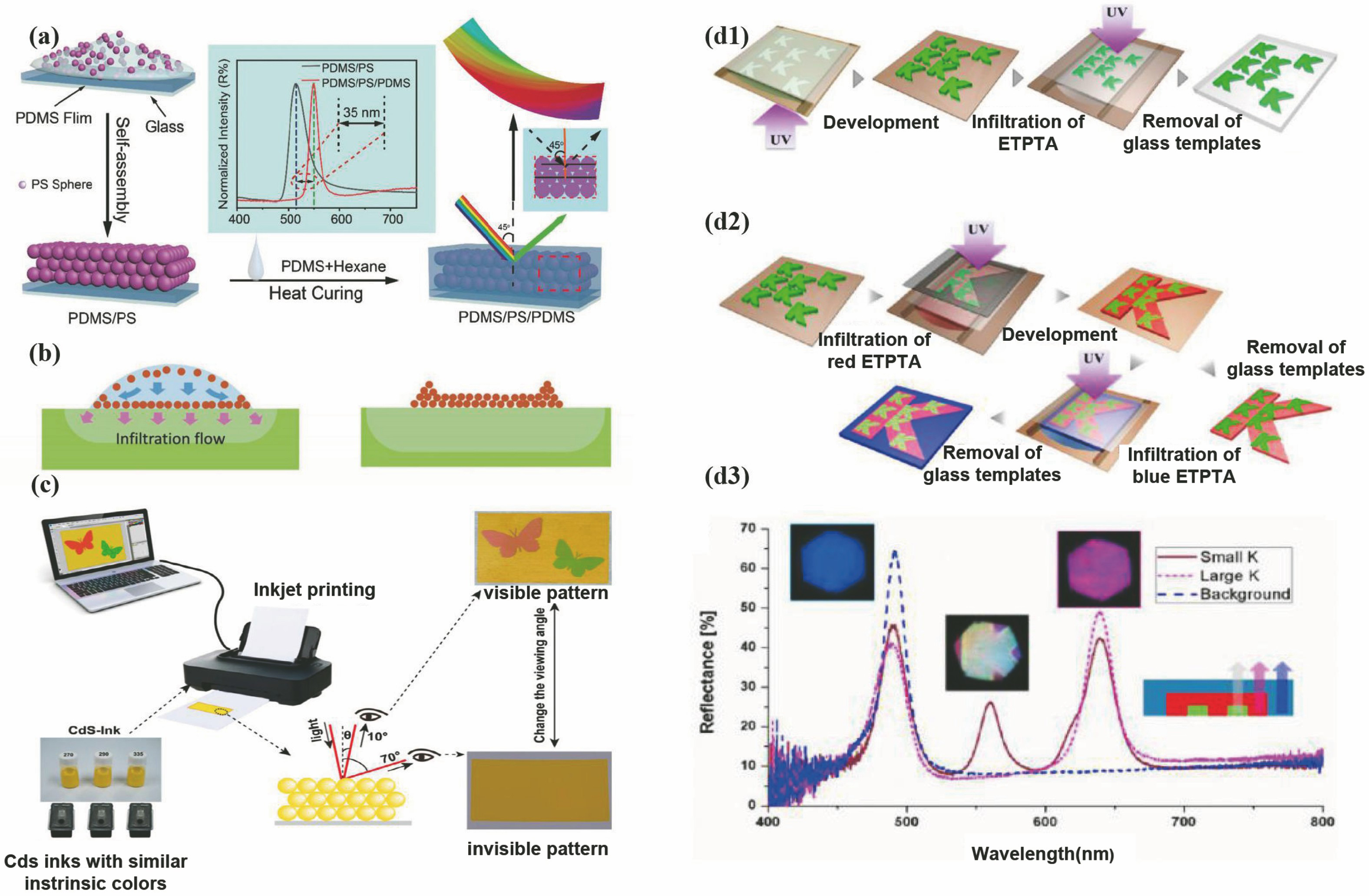
图 4. 不同入射角度下在不同基底上形成类蛋白石结构的全息图。(a)~(c)硅片;(d)(e)玻璃片;(f)(g)光面相纸[44]
Fig. 4. Holograms of opal-like structures formed on different substrates under different incident angles. (a)-(c) Silicon wafer; (d) (e) glass slide; (f) (g) glossy photo paper[44]
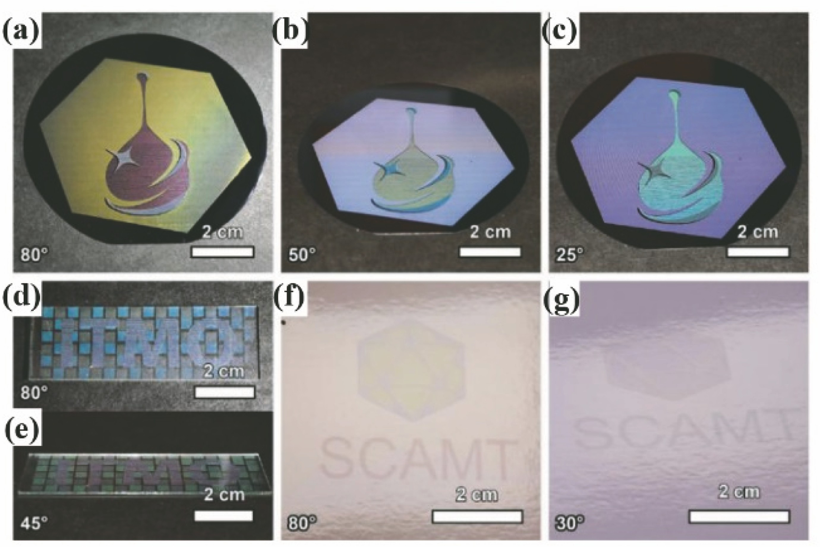
图 5. 抗反射涂层的相关工艺。(a) UT-SOI(ultrathin silicon on insulator)样品组成图及其制造流程[46];(b) TiO2层制备流程图[47];(c1)理想等离子体吸收剂的示意图[48];(c2) Au颗粒自组装形成等离子体吸收体[48];(c3)纳米多孔模板样品和Au/NPT样品图像[48];(d)介电纳米球太阳能电池的示意图[49]
Fig. 5. Fabrication processes related to anti-reflective coating. (a) Sample of UT-SOI and fabrication process[46]; (b) fabrication process of TiO2 layer[47]; (c1) schematic of ideal plasmonic absorber[48]; (c2) self-assembly of gold nanoparticles to form plasmonic absorbers[48]; (c3) images of n

图 6. 发光二极管的结构与发光效率。(a1) InGaN量子阱LED原理图[50];(a2) InGaN量子阱LED的光输出功率与电流的关系[50];(b1)超晶格作为LED背反射器的示意图[35];(b2)(b3)光输出功率和电致发光光谱[35]
Fig. 6. Structure and luminous efficiency of LEDs. (a1) Principle of InGaN quantum well LED[50]; (a2) light output power as a function of current for InGaN quantum well LED [50]; (b1) schematic of LED bottom reflector with superlattice[35]; (b2) (b3) light output power and electro-luminescence spectra[35]

图 7. 微透镜阵列制备。(a)纳米球光刻法批量化制备微透镜阵列的工艺流程[55];(b1)旋涂有PS纳米球掩模的4 inch玻璃基底[55];(b2)~(b4)不同观测尺度下的微透镜阵列[55];(c1)模拟光场分布[55];(c2)实际光场分布 [55]
Fig. 7. Fabrication of microlens arrays. (a) Schematic of mass production of microlens array by nanosphere lithography[55]; (b1) diffraction image of fabricated 4-inch glass substrate coated with PS nanosphere mask[55]; (b2)-(b4) optical microscope images of microlens array at different observation scales[55]; (c1) simulated light-field distribution[<
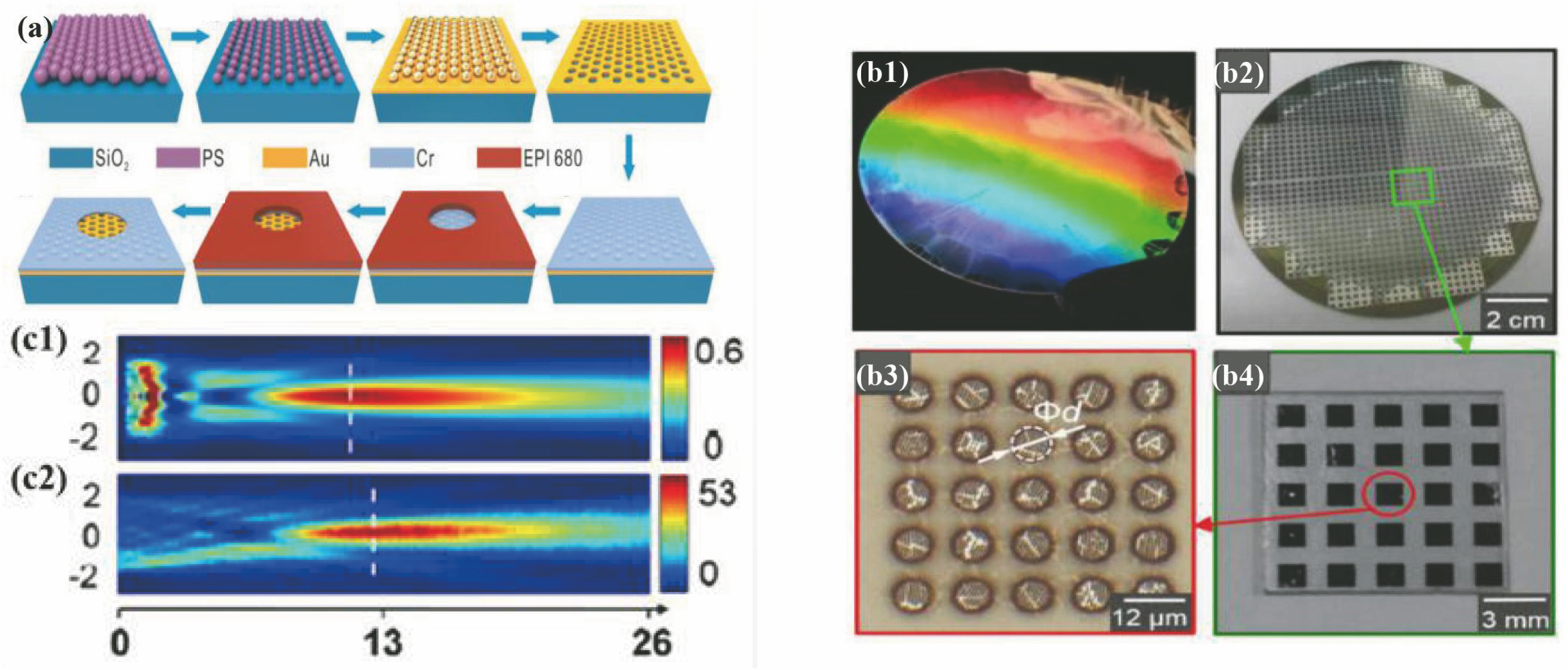
图 8. 胶体晶体激光器。(a)低阈值胶体晶体激光器原理图[56];(b)不同偏置方向电压下光子带隙偏移的示意图[57]
Fig. 8. Colloidal-crystal laser. (a) Principle of low-threshold colloidal-crystal laser[56]; (b) schematics of photonic band gap shift under voltages in different bias directions[57]
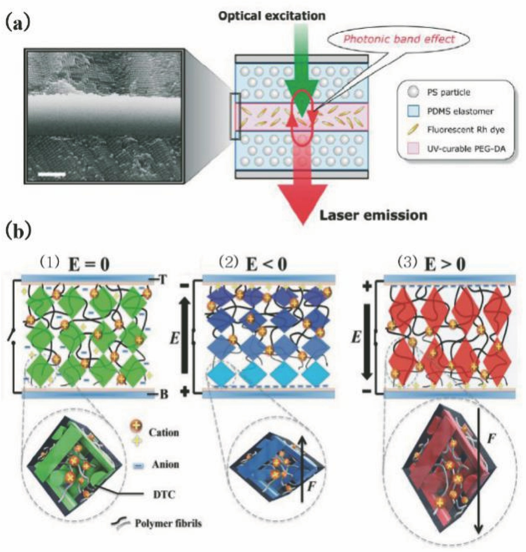
图 9. 传感器制造工艺。(a)仿生Si3N4基底的微纳工艺流程[65];(b)自组装工艺图及光纤末端的SEM图像[66];(c)拉曼检测示意图[67]
Fig. 9. Fabrication process of sensors. (a) Micro-nano fabrication process flow of bio-inspired Si3N4-membrane[65]; (b) schematic of self-assembly process and SEM image of fiber end[66]; (c) schematic of Raman measurement[67]

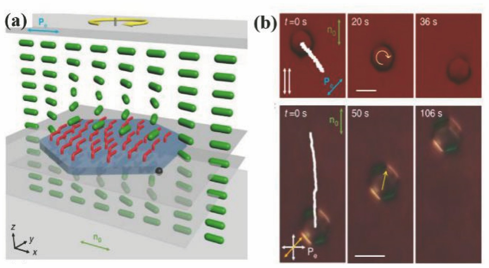
图 10. 自组装胶体马达。(a)光驱动自组装胶体马达的三维示意图,xz 平面的棒状分子为液体晶体分子,xy 平面的小棒状分子为偶氮苯分子[68];(b)偏振蓝光和偏振白光下血小板的平移运动[68]
Fig. 10. Self-assembled molecular-colloidal motor. (a) Three-dimensional schematic of self-assembled molecular-colloidal light-driven motor. Rods in xz plane represent liquid crystal molecules and, and rods in xy plane represent azobenzene molecules[68]; (b) snapshots of translational motion of platelet under polarized blue light and polarized white light[68]
谢洪洋, 余晓畅, 高麒淦, 苏扬, 孙梓翔, 虞益挺. 自组装胶体晶体在微纳光学领域的研究进展[J]. 激光与光电子学进展, 2019, 56(23): 230001. Hongyang Xie, Xiaochang Yu, Qigan Gao, Yang Su, Zixiang Sun, Yiting Yu. Self-Assembled Colloidal Crystals in Field of Micro-Nano Optics[J]. Laser & Optoelectronics Progress, 2019, 56(23): 230001.


 PDF全文
PDF全文

