激光与光电子学进展, 2019, 56 (20): 202409, 网络出版: 2019-10-22
表面等离子激元纳米激光器综述  下载: 2325次
Surface Plasmon Polariton Nanolasers
图 & 表
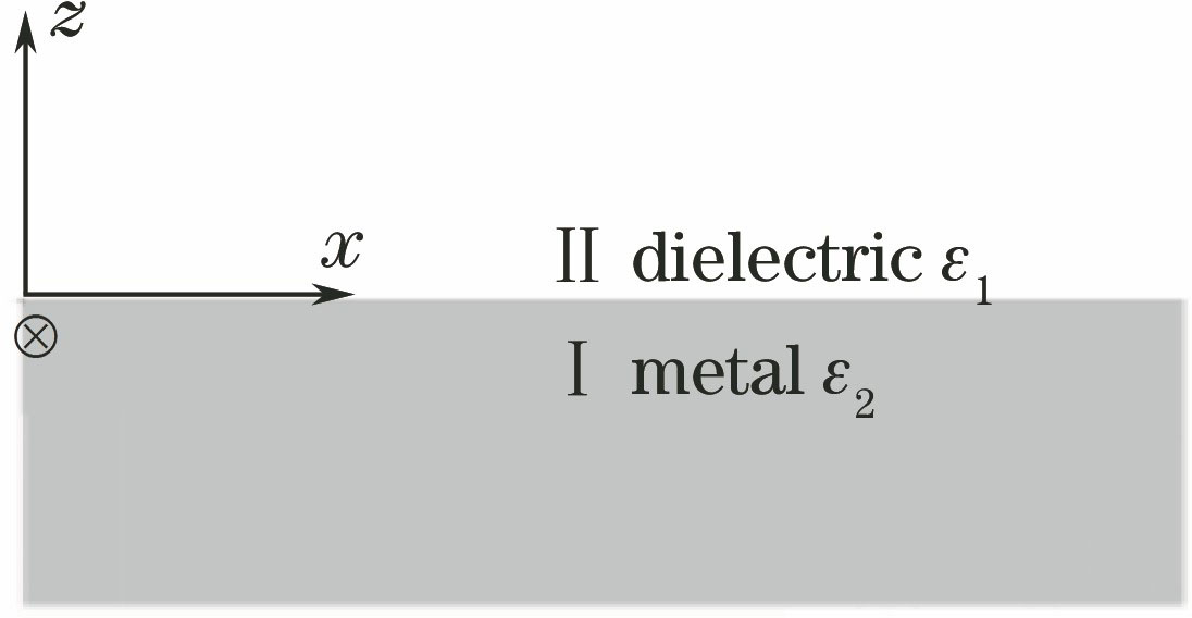
图 2. 纳米粒子表面等离子激元激光器。(a)混合纳米颗粒结构图;(b)金核的透射电子显微镜(TEM)图;(c) Au/二氧化硅/染料壳的扫描电子显微镜(SEM)图;(d)表面等离子体模式;(e)光谱结果
Fig. 2. Nanoparticle SPP laser. (a) Structural diagram of hybrid nanoparticle; (b) transmission electron microscope (TEM) image of Au core; (c) scanning electron microscope (SEM) image of Au/silica/dye core-shell; (d) surface plasmon mode; (e) spectroscopic results

图 3. 深亚波长表面等离子激元激光器。(a)器件结构图(Ag/MgF2/CdS);(b)混合等离子体模式的受激电场分布
Fig. 3. Deep subwavelength SPP laser. (a) Structural diagram of device (Ag/MgF2/CdS); (b) stimulated electric field distribution of hybrid plasmonic mode

图 4. 纳米棒表面等离子激元激光器。(a)器件结构图(Ag/SiO2/InGaN/GaN);(b)纳米棒横截面的SEM图;(c)纳米棒的扫描透射电子显微镜(STEM)图和TEM图
Fig. 4. Nanorod SPP laser. (a) Structural diagram of device (Ag/SiO2/InGaN/GaN); (b) SEM image of cross section of nanorod; (c) scanning transmission electron microscope (STEM) and TEM images of nanorod

图 5. 等离子体紫外激光器。(a) Al基纳米激光器的SPP模式色散曲线;(b) Ag基纳米激光器的SPP模式色散曲线;(c)(d)纳米激光器内部SPP模式的电场分布
Fig. 5. Plasmonic ultraviolet laser. (a) Dispersion curve of SPP modes of Al-based nanolaser; (b) dispersion curve of SPP modes of Ag-based nanolaser; (c)(d) electric field distributions of SPP modes inside nanolasers

图 6. 室温下椭圆形单模激光器。(a)器件结构示意图;(b) InGaN/GaN纳米棒的SEM图;(c)上述结构的受激电场分布;(d)不同光抽运强度下的PL光谱图(插图为490 nm处主要激光峰值的FWHM和相应的L-L曲线)
Fig. 6. Single-mode elliptical laser at room temperature. (a) Structural diagram of device; (b) SEM image of InGaN/GaN nanorod; (c) stimulated electric field distribution of above structure; (d) PL spectra under different optical pumping intensities (inset: FWHM of dominant lasing peak at 490 nm and corresponding L-L curve)

图 7. 室温下椭圆形多模激光器。(a)器件结构示意图;(b) InGaN/GaN纳米棒的SEM图;(c)等离子体模式和(d) HE11模式的受激电场分布;(e)不同光抽运强度下的PL光谱图(内嵌图为493 nm处激光峰值的L-L曲线和FWHM图)
Fig. 7. Elliptical multimode laser at room temperature. (a) Structural diagram of device; (b) SEM image of InGaN/GaN nanorod; stimulated electric field distributions of (c) plasmonic mode and (d) HE11 mode; (e) PL spectra under different optical pumping intensities (inset: corresponding L-L curve and FWHM of lasing peak at 493 nm)

图 8. 低温电抽运圆柱形金属纳米腔激光器。(a)器件结构示意图;(b)纳米柱的SEM图;(c)激光器中的光场分布
Fig. 8. Cryogenic electrically-pumped cylindrical metal nano-cavity laser. (a) Structural diagram of device; (b) SEM image of nanocolumn; (c) optical field distribution in laser

图 9. 室温光抽运圆柱形金属纳米腔激光器。(a)器件结构示意图;(b) TE012电场模式的截面图
Fig. 9. Optically-pumped cylindrical metal nano-cavity laser at room temperature. (a) Structural diagram of device; (b) cross-sectional view of TE012 electric field mode

图 10. 等离子体纳米粒子腔结构。(a)纳米圆盘/纳米颗粒结构示意图;(b)银孔示意图(从上至下分别对应于玻璃、InP和银);(c)镀银之前在玻璃上的InP盘SEM图;(d)从圆盘中分离出的银膜的SEM图
Fig. 10. Structure of plasmonic nanoparticle cavity. (a) Structural diagram of nanodisk/nanoparticle structure; (b) schematic of silver hole (corresponding to glass, InP disk, and silver from top to bottom); (c) SEM image of InP disk on glass before silver plating; (d) SEM image of silver film separated from disk

图 11. 纳米片半导体激光器的结构和模式分布。(a)金属电介质纳米片半导体激光器的结构示意图;(b)器件的SEM图;(c)电偶极模式模场图;(d)二阶磁偶极模式模场图
Fig. 11. Structure and mode distributions of nanopatch semiconductor laser. (a) Structural diagram of metal-dielectric nanopatch semiconductor laser; (b) SEM image of device; (c) mode field profile for electrical dipole mode (TM111); (d) mode field profile for second-order magnetic dipole mode (TE011)

图 12. 金属-介质-金属结构纳米激光器。(a)InP基-介质-金属脊形纳米激光器示意图;(b)激光光谱和近场模式(插图是78 K下抽运电流分别为20(1),40(2),60(3) μA时的发射光谱图)
Fig. 12. Metal-dielectric-metal structure nanolaser. (a) Schematic of InP substrate-medium-metal ridge-like nanolaser; (b) spectra and near field patterns of laser, (inset: emission spectra for pump currents of 20(1), 40(2), and 60(3) μA at 78 K)

图 13. Si波导耦合金属包覆纳米激光腔。(a)透视图;(b)(c)截面图
Fig. 13. Si waveguide coupled metal-clad nanolaser cavity. (a) Perspective; (b)(c) cross-sectional diagrams

图 14. 石墨烯纳米激光器。(a) SPP波导的二维结构图;(b)激光器电场分布图
Fig. 14. Graphene nanolaser. (a) Two-dimensional structure of SPP waveguide; (b) electric distribution of laser

图 15. 基于W-G效应的室温表面等离子激元激光器。(a)室温下SPP激光器示意图;(b) TM模式在x和y方向上的电场强度分布;(c)非对称结构激光模式的电场分布图;(d)激光光谱及光抽运响应(曲线1、2、3分别对应自发辐射、放大自发辐射和全激光振荡);(e)非对称结构的激光光谱及集成光抽运响应(曲线1、2、3分别对应自发辐射、放大自发辐射和全单模激光振荡)
Fig. 15. Room-temperature SPP laser based on W-G effect. (a) Schematic of room-temperature SPP laser; (b) electric-field-intensity distribution of TM mode in x and y direction; (c) electric field distribution of asymmetric structure laser mode; (d) laser spectra and optical pumping response (curves 1, 2 and 3 correspond to spontaneous emission, amplified spontaneous emission, and full laser oscillation, respectively); (e) laser spectra and integrated light-pump response of anti-symmetric structure (curve

图 16. 倒置楔形二氧化硅谐振器。(a)谐振器结构示意图;(b)边缘横截面放大图;(c)~(i) rt=30 μm和hg=2 μm时微腔中不同回音壁模式的能量密度分布
Fig. 16. Inverted-wedge silica resonator. (a) Structural diagram of resonator; (b) magnified diagram of cross-section of edge; (c)-(i) energy density distributions of different whispering gallery modes in microcavities with rt=30 μm and hg=2 μm


杨琳, 段智勇, 马刘红, 李梦珂. 表面等离子激元纳米激光器综述[J]. 激光与光电子学进展, 2019, 56(20): 202409. Lin Yang, Zhiyong Duan, Liuhong Ma, Mengke Li. Surface Plasmon Polariton Nanolasers[J]. Laser & Optoelectronics Progress, 2019, 56(20): 202409.


 PDF全文
PDF全文

