Photonics Research, 2020, 8 (8): 08001388, Published Online: Jul. 31, 2020
Impact of carrier transport on the performance of QD lasers on silicon: a drift-diffusion approach  Download: 626次
Figures & Tables
Fig. 1. Schematic representation of the epitaxial structure of the studied QD lasers, similar to those in Refs. [24,25]. The growth direction is from the bottom to the top.
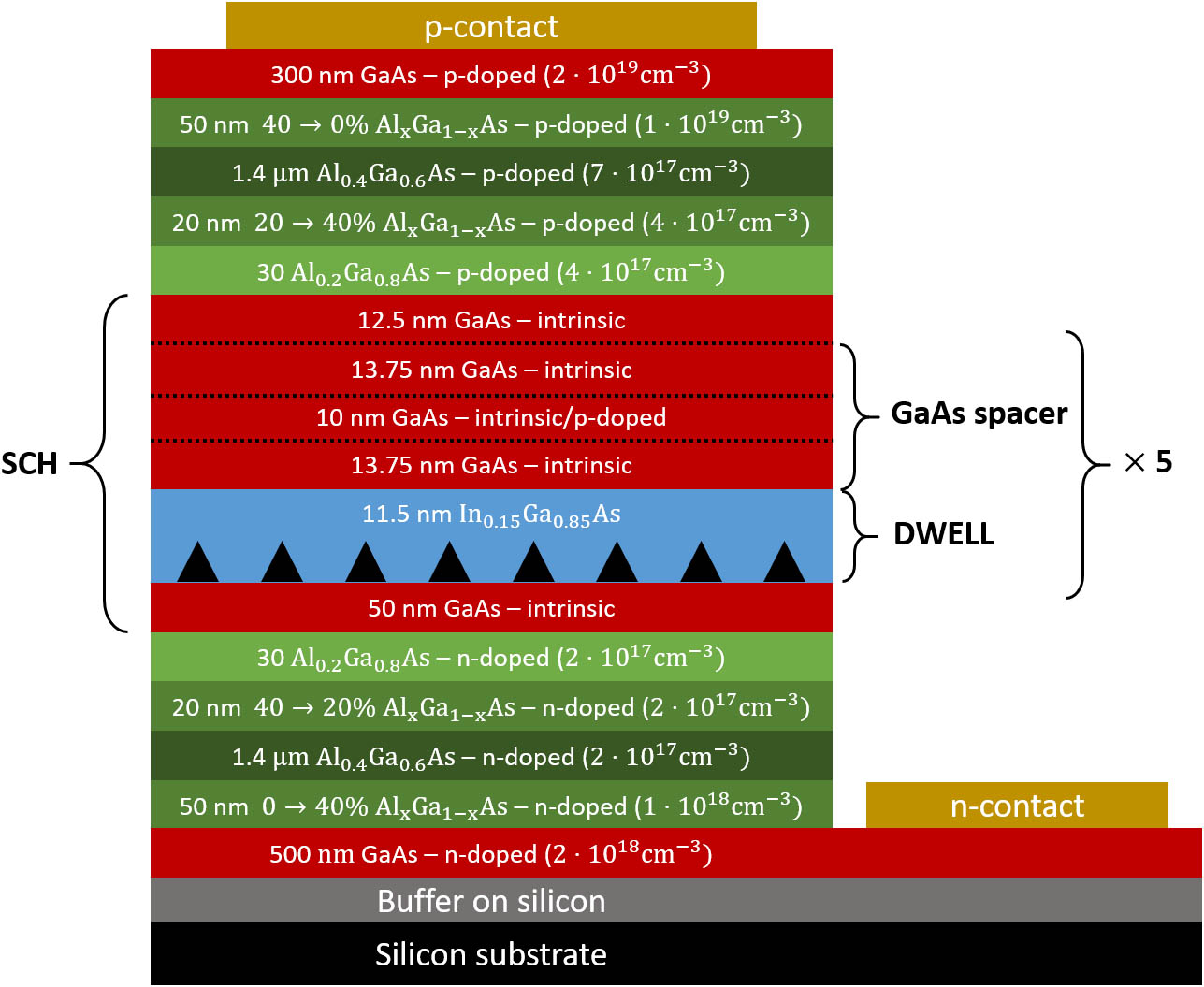
Fig. 2. Band diagram at thermodynamic equilibrium, with the conduction band (blue), the valence band (red), and the Fermi level (dashed, black). The dotted, vertical lines delimit the SCH region.


Fig. 4. Calculated GS modal gain versus current density for different levels of TDD and experimental gain (circles) from Ref. [24].

Fig. 5. (a) GS threshold current density and (c) optical power as a function of TDD bulk TDD WL = 10 5 cm − 2 TDD WL = TDD bulk

Fig. 6. GS (solid) and ES (dotted) optical power with (a) μ n = 8500 cm 2 / ( V · s ) μ p = 350 cm 2 / ( V · s ) μ n = μ p = 8500 cm 2 / ( V · s )

Fig. 7. Net capture rate from the bulk states to the WL with (a) μ n = 8500 cm 2 / ( V · s ) μ p = 350 cm 2 / ( V · s ) μ n = μ p = 8500 cm 2 / ( V · s )

Fig. 8. Contribution of (a) electrons and (b) holes to the GS modal gain: solid line is the overall contribution, whereas colored dashed lines are the contribution of the different layers (color legend is the same as in Fig. 6 ). Vertical lines indicate GS and ES threshold currents. (c) GS electrons and (d) holes occupation probability. The mobility of electrons and holes in the SCH region is μ n = 8500 cm 2 / ( V · s ) μ p = 350 cm 2 / ( V · s )

Fig. 9. GS (solid) and ES (dotted) optical power with (a) no p-type modulation doping and a p-type modulation doping of (b) 5 × 10 17 cm − 3 30 × 10 17 cm − 3

Fig. 10. (a) GS (blue) and ES (red) threshold current density as functions of the p-type modulation doping density. (b) Total radiative and SRH recombination rates as functions of p-type modulation doping density calculated at the J th GS

Fig. 11. (a) GS modal gain versus current density and (b) holes (G GS mod , p G GS mod , n

Fig. 12. (a) Contribution of electrons (blue) and holes (red) to the GS modal gain at J = 580 A / cm 2

Fig. 13. (a) Conduction band (solid) and electron quasi-Fermi level (dashed) for the bulk states of the SCH region at J = 580 A / cm 2 J = 580 A / cm 2

Fig. 14. Net capture rate from the bulk states to the WL at J = 580 A / cm 2


Table1. Simulation Parameters
|
Marco Saldutti, Alberto Tibaldi, Federica Cappelluti, Mariangela Gioannini. Impact of carrier transport on the performance of QD lasers on silicon: a drift-diffusion approach[J]. Photonics Research, 2020, 8(8): 08001388.


 PDF全文
PDF全文

