全息波导耦合元件对称结构的研究  下载: 1036次
Research on Symmetric Structure of Holographic Waveguide Coupling Elements
西安工业大学光电工程学院, 陕西 西安 710021
图 & 表
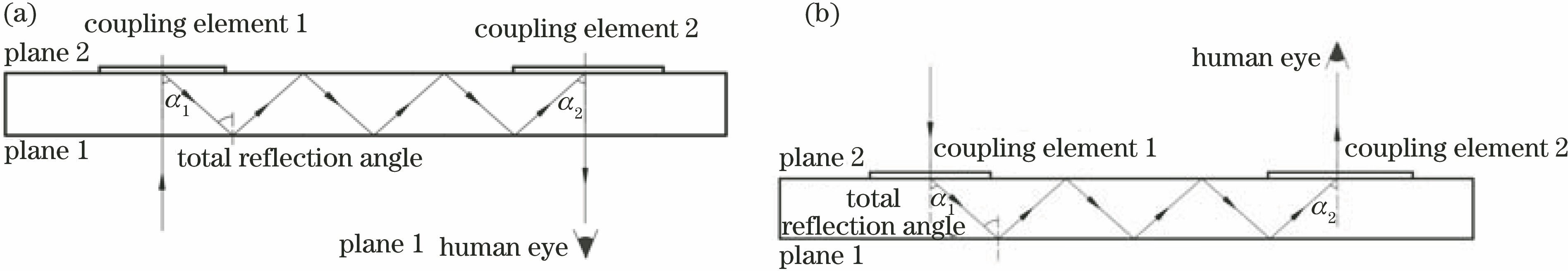
图 1. 全息波导板光路传输示意图。(a)反射式耦合元件;(b)透射式耦合元件
Fig. 1. Schematic of holographic waveguide plate optical path transmission. (a) Reflection coupling elements; (b) transmission coupling elements
下载图片 查看原文
图 2. 透射式耦合元件记录与再现示意图。(a)耦合元件1记录示意图;(b)耦合元件2记录示意图;(c)耦合元件1再现示意图;(d)耦合元件2再现示意图
Fig. 2. Schematic of recording and reproduction of transmissive coupling element. (a) Schematic of coupling element 1 recording; (b) schematic of coupling element 2 recording; (c) schematic of coupling element 1 reproduction; (d) schematic of coupling element 2 reproduction
下载图片 查看原文
图 3. 反射式耦合元件的光栅矢量分析图。(a)耦合元件1的K矢量圆分析图;(b)耦合元件1的光栅倾角示意图;(c)耦合元件2的K矢量圆分析图;(d)耦合元件2的光栅倾角示意图
Fig. 3. Grating vector analysis diagram of projective coupling elements. (a) K vector circle analysis diagram of coupling element 1; (b) schematic of grating inclination of coupling element 1; (c) K vector circle analysis diagram of coupling element 2; (d) schematic of grating inclination of coupling element 2
下载图片 查看原文
图 4. 透射式耦合元件的光栅矢量分析图。(a)耦合元件1的K矢量圆分析图;(b)耦合元件1的光栅倾角示意图;(c)耦合元件2的K矢量圆分析图;(d)耦合元件2的光栅倾角示意图
Fig. 4. Grating vector analysis diagram of projective coupling elements. (a) K vector circle analysis diagram of coupling element 1; (b) schematic of the grating inclination of the coupling element 1; (c) K vector circle analysis diagram of coupling element 2; (d) schematic of the grating inclination of the coupling element 2
下载图片 查看原文
图 5. 耦合元件记录光路示意图。(a)透射式耦合元件1;(b)透射式耦合元件2;(c)反射式耦合元件1;(d)反射式耦合元件2
Fig. 5. Schematic of coupling element recording optical path. (a) Transmissive coupling element 1; (b) transmissive coupling element 2; (c) reflective coupling element 1; (d) reflective coupling element 2
下载图片 查看原文
图 6. 耦合元件在记录时的干涉光强仿真结果。(a)透射式耦合元件1;(b)透射式耦合元件2,(c)反射式耦合元件1;(d)反射式耦合元件2
Fig. 6. Interference light intensity simulation result of coupling element during recording. (a) Transmissive coupling element 1; (b) transmissive coupling element 2; (c) reflective coupling element 1; (d) reflective coupling element 2
下载图片 查看原文
图 7. 耦合元件再现时的截面电场分布仿真结果。(a)透射式耦合元件1;(b)透射式耦合元件2;(c)反射式耦合元件1;(d)反射式耦合元件2
Fig. 7. Simulation results of cross-sectional electric field distribution when the coupling element is reproduced. (a) Transmissive coupling element 1; (b) transmissive coupling element 2; (c) reflective coupling element 1; (d) reflective coupling element 2
下载图片 查看原文
图 8. 波长偏移量对光栅常数和一级衍射角的影响。(a)光栅常数;(b)一级衍射角
Fig. 8. Influence of wavelength shift on grating constant and first-order diffraction angle. (a) Grating constant; (b) first-order diffraction angle
下载图片 查看原文
表 1透射式耦合元件的光栅结构与入射光参数
Table1. Grating structure and incident light parameters of transmissive coupling element
| Coupling element | Wavelength /nm | Grating constant /nm | Grating angle /(°) | Incident light angle /(°) |
|---|
| 1 | 633 | 589 | 21 | 0 | | 2 | 633 | 589 | -21 | -42 |
|
查看原文
表 2反射式耦合元件的光栅结构与入射光参数
Table2. Grating structure and incident light parameters of reflective coupling element
| Coupling element | Wavelength /nm | Grating constant /nm | Grating angle /(°) | Incident light angle /(°) |
|---|
| 1 | 633 | 226 | -69 | 0 | | 2 | 633 | 226 | 69 | -42 |
|
查看原文
表 3透射式耦合元件一级衍射光方向参数
Table3. First-order diffracted light direction parameter of transmissive coupling element
| Coupling element | Vector x | Vector y | First orderdiffraction angle /(°) | Ideal first orderdiffraction angle /(°) |
|---|
| 1 | 9294652.82 | 8569437.29 | 42.00 | 42 | | 2 | 47310.22 | -1.38×10⁷ | 0.00 | 0 |
|
查看原文
表 4反射式耦合元件一级衍射光方向参数
Table4. First-order diffracted light direction parameter of reflective coupling element
| Coupling element | Vector x | Vector y | First orderdiffraction angle /(°) | Ideal first orderdiffraction angle /(°) |
|---|
| 1 | -9962556.78 | 1.11×10⁷ | 42.00 | 42 | | 2 | -172.12 | 1.49×10⁷ | 0.00 | 0 |
|
查看原文
王玉瑾, 张锦, 蒋世磊, 孙国斌, 季雪淞. 全息波导耦合元件对称结构的研究[J]. 激光与光电子学进展, 2020, 57(15): 152303. Yujin Wang, Jin Zhang, Shilei Jiang, Guobin Sun, Xuesong Ji. Research on Symmetric Structure of Holographic Waveguide Coupling Elements[J]. Laser & Optoelectronics Progress, 2020, 57(15): 152303.


 PDF全文
PDF全文

