1. INTRODUCTION
Infrared (IR) spectroscopy is often considered as a gold standard in analytical chemistry given its ability to unequivocally identify chemical species via “fingerprinting” the molecular vibrational modes. Traditionally, IR spectroscopy relies on benchtop instruments only available in a dedicated laboratory setting. In recent years, integrated photonics has emerged as a promising solution to liberate the technology from the constraint by potentially enabling sensor integration on chip-scale platforms [1–8" target="_self" style="display: inline;">–8]. These early demonstrations make use of tunable lasers to perform wavelength interrogation and identify spectral signatures of target molecules. However, the use of tunable lasers, which are bulky instruments involving complex mechanical moving parts, is counterproductive to compact sensing system integration. Moreover, the laser tuning range is bound by gain bandwidth of the lasing medium, which is often merely a small fraction of an octave. Using current or temperature ramping for laser wavelength tuning offers a viable option for miniaturized light sources [9], although the accessible spectral domain using these techniques is small. Consequently, such sensors are limited to the detection of one single species and can be prone to interferences.
In this paper, we report, to the best of our knowledge, the first demonstration of an on-chip spectroscopic chemical sensor with a monolithically integrated supercontinuum (SC) light source. Unlike traditional broadband blackbody sources used in benchtop IR spectrophotometers, waveguide SC sources feature high spatial coherency essential for efficient light coupling and manipulation on a photonic chip. Compared to tunable lasers, SC offers superior bandwidth coverage: for instance, waveguide SC spanning three octaves has been experimentally realized [10]. The broadband nature of SC facilitates access to wavelengths difficult to cover using semiconductor lasers and thereby significantly expands the identifiable molecule repertoire of spectroscopic sensors. In our experiment we use chalcogenide glass (ChG) as the waveguide material for both SC generation and evanescent wave sensing. ChGs are known for their broadband infrared transparency, large Kerr nonlinearity, and low two photon absorption (TPA), ideal characteristics for our application [11,12]. Indeed, ChG waveguides have been separately applied to broadband SC generation [13–17" target="_self" style="display: inline;">–17] and IR spectroscopic sensing [18–24" target="_self" style="display: inline;">–24]. Here we combine for the first time both functions in a single chip-scale platform, allowing the on-chip photonic sensor to interrogate a broad spectral region from 1.38 to 2.05 μm not accessible with a single tunable laser. In addition, unlike previous SC generation experiments in ChGs where bulky pulsed pump lasers were used, we employed a home-built, palm-sized femtosecond laser as the pump source. The laser uses a graphene saturable absorber in an all-fiber system to realize passive mode-locking, and the entire laser can be integrated in a small module of a few centimeters in size [25]. Our work here therefore envisions a standalone, compact spectroscopic sensing system once coupled with miniaturized chip-scale spectrometers we recently developed [2628" target="_self" style="display: inline;">–28].
2. EXPERIMENTAL DESIGNS AND SETUP
2.1 A. Designs and Fabrication of GeSbSe Waveguides
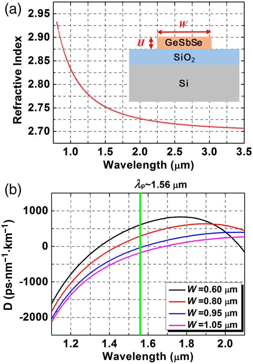
Films of 400 nm thick (GeSbSe) were thermally evaporated onto 4” silicon wafers with 3 μm thermal oxide as an undercladding from GeSbSe glass powder (prepared by melt quenching in a quartz ampoule). Stoichiometry of the film was confirmed by wavelength dispersion X-ray spectroscopy (JEOL-JXA-8200 Superprobe WDS) at 5 different locations on each sample to confirm its compositional uniformity. We choose this glass composition given its large optical nonlinearity (nonlinear index ) and low TPA (TPA coefficient ), both measured using the Z-scan technique at 1550 nm wavelength. The GeSbSe glass therefore exhibits a nonlinear figure of merit (defined as , where is the wavelength) of 8.3, over one order of magnitude larger than that of silicon at the same wavelength [29]. Refractive index dispersion of the glass film was characterized using Woollam V-VASE32 ellipsometry and plotted in Fig. 1(a). The data were then used to compute the group velocity dispersion (GVD) of the fundamental quasi-TE mode in GeSbSe waveguides with varying widths [Fig. 1(b)]. As seen in Fig. 1(b), as waveguide width increases from 0.6 to 1.05 μm, the zero-dispersion wavelength progressively shifts towards longer wavelength from 1.35 to 1.68 μm. To efficiently excite SC in a waveguide, the pump wavelength should be located near the zero-dispersion wavelength. Therefore, the optimal GeSbSe waveguide dimensions are with a zero-dispersion wavelength at 1.56 μm, our pump central wavelength.
Fig. 1. (a) Refractive index dispersion of the glass film measured using ellipsometry; inset schematically depicts the waveguide structure. (b) Simulated GVD of GeSbSe waveguides with varying widths () and a fixed core thickness .
下载图片 查看所有图片
GeSbSe waveguides with varying widths were fabricated using our previously established protocols [30]. In the process, a 350-nm-thick ZEP resist layer was spun onto the substrate followed by exposure on an Elionix ELS-F125 tool at a beam current of 10 nA. The resist pattern was then developed by immersing in ZED-N50 developer for 1 min. Reactive ion etching was performed in a PlasmaTherm etcher to transfer the resist pattern to the glass layer. The etching process used a gas mixture of and at 3:1 ratio and 5 mTorr total pressure. The incident radio frequency (RF) power was fixed at 200 W. Finally, the device was immersed in -methyl-2-pyrrolidone (NMP) overnight to remove the ZEP resist and complete device fabrication. The waveguides assume a zigzag geometry with length up to 21 mm [Fig. 2(a)]. A cross-sectional scanning electron electrode (SEM) image of the waveguide is displayed in Fig. 2(b), showing vertical sidewalls free of etching residue.
Fig. 2. (a) Top-view optical micrograph of the zigzag GeSbSe waveguides; (b) SEM cross-sectional image of a GeSbSe waveguide. (c) Experimental setup of on-chip SC generation and sensing. (d) Block diagram of home-built femtosecond laser module (OC, optical coupler; WDM, wavelength division multiplexer; SA, graphene saturable absorber; PC, polarization controller).
下载图片 查看所有图片
2.2 B. Experimental Setup for SC Generation and Sensing
The waveguides were tested for SC generation using a setup schematically illustrated in Fig. 2(c). The pump source is a home-built, palm-sized femtosecond laser module [Fig. 2(d)] with a central wavelength of 1560 nm, a repetition rate of 8.1 MHz, and a pulse duration of 800 fs [25]. The laser is assembled on an all-fiber platform and passively mode-locked using a graphene saturable absorber synthesized in-house [31]. The femtosecond seed laser was then amplified by a homemade erbium-doped fiber amplifier (EDFA) to boost the average power from 0.2 mW to a maximum of 5.5 mW, producing a peak power of approximately 0.8 kW after amplification. The fibers used in our experiment can be easily spooled to a centimeter-scale radius with negligible bending loss. Therefore, the all-fiber construction of the laser and amplifier potentially allows the light source module to be further downscaled to an ultra-compact package of a few centimeters in size. The TE-polarized amplified pulses were coupled into and out of the GeSbSe waveguide devices via taper lensed fibers with a coupling loss of approximately 7 dB per facet. An optical spectrum analyzer (OSA, Yokogawa AQ6375B, covering 1.2–2.4 μm wavelength range) was used to spectrally resolve output light from the chip. By replacing the OSA with an on-chip spectrometer (for example, the digital Fourier transform spectrometer we recently developed [8]), we may realize a compact handheld sensing system.
3. EXPERIMENTAL RESULTS AND DISCUSSIONS
Next we investigated the influence of waveguide geometry, waveguide length, and pump power on the SC spectra to elucidate the SC generation mechanism and understand sensor device design trade-offs. Figure 3(a) presents the SC spectra in GeSbSe waveguides of different widths. All the waveguides have the same core thickness of 0.4 μm and a uniform length of 21 mm. SC generated by the waveguide with a 0.95 μm width, whose zero-dispersion point aligns with the pump wavelength, exhibits the maximum bandwidth consistent with our GVD simulations. For waveguides with widths and 0.8 μm, the pump wavelength is largely away from their zero-dispersion wavelengths. In this regime, SC is formed through initial self-phase modulation followed by self-steepening and other high-order nonlinear effects contributing to spectral broadening. In contrast, for waveguides with and 1.05 μm, the pump wavelength is located near the zero-dispersion point. In this case, a broad SC spectrum results from soliton fission, self-frequency shift, and dispersive wave emission [13]. To further validate the SC generation mechanism, we compute the nonlinear length (, where and denote the pump peak power and waveguide nonlinear parameter, respectively) to be 0.29 mm, which is almost one order of magnitude smaller than the waveguide length. Therefore, we conclude that the SC generation mechanism in our device is dominated by high-order soliton fission from various kinds of nonlinear optical effects.
Fig. 3. SC spectra in GeSbSe waveguides: (a) SC spectra from waveguides with different widths ; when , the zero-dispersion point of the waveguide coincides with the pump wavelength; (b) SC generation of GeSbSe waveguides with the optimal geometry (, ) and varying lengths; (c) SC spectra from a 21 mm long GeSbSe waveguide (, ) at different pump power levels. The power quoted here represents the average optical power coupled into the waveguide.
下载图片 查看所有图片
Figure 3(b) plots the SC spectra in GeSbSe waveguides with the different lengths and the optimal dimensions (, ). As indicated in the figure, the SC bandwidth extends to over half an octave, albeit with decreased total output power when the waveguide length increases to 21 mm. This power attenuation is attributed to the GeSbSe waveguide propagation loss, measured using the cut-back method to be . This trade-off between SC spectral coverage and power can be mitigated with reduced waveguide losses.
SC spectra from the 21-mm-long waveguide (, ) are shown in Fig. 3(c) for several pump power levels. Clearly, higher pump power produces SC with an increased bandwidth. The maximum SC spectral span we obtained in our experiment is 1380 to 2050 nm (gauged at 20 dB flatness), primarily limited by the optical power available from our compact pump source. If desired, higher pump power and hence even wider SC spectral coverage can be obtained by adding more amplification stages, albeit at the expense of the compactness of the system.
In the sensing experiment, the GeSbSe waveguide was immersed in carbon tetrachloride () solutions containing varying concentrations of chloroform (). The solvent is optically transparent across the near-IR [19]), whereas the C-H bond in chloroform leads to an overtone absorption peak centering at 1695 nm, a wavelength outside the standard telecommunication bands. Here we use the C-H overtone absorption to quantify the sensing performance of our device. SC spectra near the chloroform absorption peak obtained with GeSbSe waveguides of different lengths or solutions of different concentrations are presented in Figs. 4(a) and 4(b), respectively. The data were normalized to the background (collected in pure ) and the raw spectra are furnished in the inset. Figure 4(c) plots the absorption at 1695 nm versus waveguide length, indicating that the classical Lambert’s law is obeyed in the new SC-enabled sensing mechanism. The optical absorption coefficient (in dB/cm) of chloroform at 1695 nm was also quantified using a benchtop UV-Vis spectrophotometer, which is used to project the absorption (in decibel, dB) measured from the waveguide sensor [marked with a triangle in Fig. 4(a)] following
Fig. 4. (a) SC spectra measured on GeSbSe waveguides of different lengths when immersed in chloroform; the triangle marks the optical absorption at 1695 nm calibrated using a benchtop UV-Vis spectrometer for an equivalent waveguide path length ; (b) SC spectra taken on a 21 mm long GeSbSe waveguide immersed in CHCl3–CCl4 solutions of varying volume concentration ratios; (c) measured peak absorption at 1695 nm versus the GeSbSe waveguide length used in the experiment. The linear relation indicates that the classical Lambert’s law is obeyed; the inset shows the mode profile simulated by finite difference method.
下载图片 查看所有图片
Here denotes the waveguide modal confinement factor in the solution, which is 6.8% computed using a finite difference mode solver [shown in Fig. 4(c) inset]. The agreement between the two techniques suggests that the waveguide sensor can be applied to quantitative analysis of absorption coefficients in chemical samples.
4. CONCLUSION
In conclusion, we demonstrated in this work an on-chip spectroscopic sensor where a chalcogenide glass waveguide served as both the broadband SC light source and the evanescent sensing element. By incorporating highly nonlinear GeSbSe glass in a dispersion engineered waveguide design, SC spanning over half of an octave was achieved using a compact femtosecond laser pumping source. We validated the sensing performance of the device through quantifying the C-H bond overtone absorption of chloroform at 1695 nm wavelength. This prototype envisages a handheld spectroscopic sensing platform with broadband interrogation capability suitable for field-deployed applications.
5 Acknowledgment
Acknowledgment. The authors acknowledge the fabrication and characterization facility support from the Microsystem Technology Laboratory at MIT and the Center for Nanoscale Systems at Harvard. The authors also thank Nilanjan Chatterjee and Pan Wang for their assistance on WDS and UV-Vis measurements.
Qingyang Du, Zhengqian Luo, Huikai Zhong, Yifei Zhang, Yizhong Huang, Tuanjie Du, Wei Zhang, Tian Gu, Juejun Hu. Chip-scale broadband spectroscopic chemical sensing using an integrated supercontinuum source in a chalcogenide glass waveguide[J]. Photonics Research, 2018, 6(6): 06000506.
 Download: 766次


