Chinese Optics Letters, 2017, 15 (1): 010004, Published Online: Jul. 26, 2018  

Subwavelength grating waveguide devices in silicon-on-insulators for integrated microwave photonics (Invited Paper) Download: 881次

Author Affiliations
Department of Electrical and Computer Engineering, McGill University, Montreal, QC H3A 0E9, Canada
Abstract
We provide an overview of our recent work on developing subwavelength grating (SWG) waveguide devices as an enabling technology for integrated microwave photonics. First, we describe wavelength-selective SWG waveguide filters, including ring resonators, Bragg gratings, and contradirectional couplers. Second, we discuss the development of an index variable optical true time delay line that exploits spatial diversity in an equal-length waveguide array. These SWG waveguide components are fundamental building blocks for realizing more complex structures for advanced microwave photonic signal processing.

Microwave photonic (MWP) systems exploit the advantages of photonics, especially with regards to ultrabroad bandwidth, adaptability, and parallelism, characteristics that are significantly more challenging to implement in the electronic domain[13" target="_self" style="display: inline;">–3]. Thus, MWP systems can be used to realize a number of microwave signal processing functions, including, waveform generation, Hilbert transformation, and time delay/phase shifting.

Significant efforts are currently devoted toward developing integrated photonic technologies to realize MWP signal processing functions[37" target="_self" style="display: inline;">7]. This has been motivated in part by the need to address issues associated with conventional MWP systems and signal processing engines based on either fiber or bulk optics, particularly with regard to the lack of compactness, stability, and reliability. A number of MWP integration platforms have been explored (see Ref. [4] for a review) and each platform has strengths/advantages and/or disadvantages in terms of realizing passive functionality, e.g., optical signal routing or filtering, and active functionality, e.g., O/E, E/O, and integration with RF electronics.

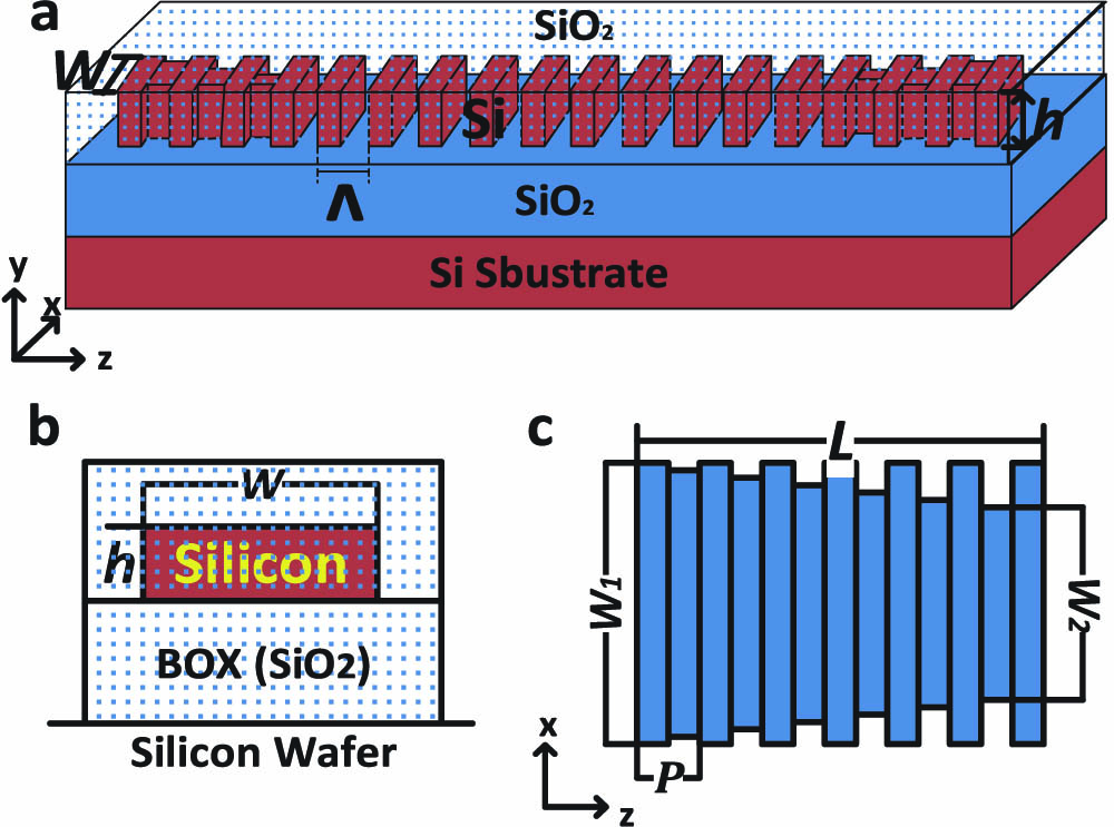
Recently, there has been growing interest in realizing integrated optical components based on subwavelength grating (SWG) structures[817" target="_self" style="display: inline;">17]. As illustrated in Fig. 1(a), SWGs are formed by a periodic arrangement (with period Λ) of a high refractive index material (e.g., silicon) with thickness a surrounded by a low refractive index material (e.g., silica); the duty cycle of the SWG is defined as D=a/Λ. Light can propagate in the direction perpendicular to the subwavelength structure, i.e., a crosswise operation, as well as parallel to the axis of the structure, i.e., a lengthwise operation. In this paper, we consider the latter case, whereby light can propagate in the SWG structure in the same way as in a conventional waveguide[8].

Fig. 1. SWG waveguide in SOI: (a) basic structure, (b) waveguide cross-section, and (c) top view of am SWG taper used to couple light between an SWG waveguide and a conventional waveguide.

下载图片 查看所有图片

To create an SWG waveguide, finite transverse dimensions, e.g., a height h and width W, are applied to a material of a high refractive index, as shown in Fig. 1(b). The carrier frequency of the incident light signal determines the operating regime of the SWG waveguide. We are particularly interested in what is known as the subwavelength regime, whereby the SWG waveguide can be modeled as a conventional waveguide having the same transverse dimensions and a uniform refractive (effective) index along the direction of propagation. The effective index of the SWG waveguide depends on the duty cycle D. Note that tapers are used to convert a waveguide mode propagating in a conventional waveguide (e.g., silicon nanowire waveguide) into a Bloch mode that propagates in the SWG waveguide. These (SWG) tapers, depicted in Fig. 1(c), are based on a linearly chirped grating structure that has a uniform period P and where the waveguide width is narrowed in a linear manner from a width W1 to W2 over a length Ltaper[12].

In this paper, we review recent work on realizing basic building blocks based on SWG waveguides in SOI that can be used to implement more complex, integrated MWP signal processing engines. This includes SWG filters such as microring resonators (MRRs), Bragg gratings (BGs), and broadband contradirectional couplers (CDCs), as well as index-variable optical true time delay lines (OTTDLs).

Various MRR-based integrated circuits have been implemented in SOI as well as silicon nitride[5]. Recently, we demonstrated both conventional MRR and racetrack ring resonators based on SWG waveguides in SOI[17].

First, we realized conventional MRRs with add–drop ports based on two SWG bus waveguides and an SWG ring waveguide, as shown in Fig. 2(a). The devices (as well as others described in this paper) were fabricated using e-beam lithography and a full etch. The waveguide dimensions are h=220nm×W=500nm. The waveguides sit on a 3 μm thick buried oxide (BOX) layer and are covered by an index-matched cladding layer of thickness 2 μm (this also applies to all other devices described in this paper). Here, the SWG grating period is Λ=300nm and the duty cycle is D=50%. A gap length g=640nm is used for coupling between the ring and bus waveguides. The SWG taper has P=200nm, and the waveguide width is reduced from 500 to 200 nm over a length Ltaper=15μm. Vertical grating couplers (VGCs) optimized for TE transmission serve to couple light into and out of the device; conventional nanowire waveguides in SOI connect the VGCs to the SWG waveguides (via the SWG tapers). The typical fiber-to-fiber loss of an MRR is 16dB; sources of loss include coupling loss due to the VGCs used for input and output coupling, propagation loss in the SWG waveguide (including bending loss), and insertion loss from the SWG tapers used for coupling between conventional nanowire and SWG waveguides (due to mode mismatch). Figures 2(c)2(e) show the measured through responses for SWG MRRs with different ring radii. Our MRRs exhibit Q-factors of several hundred to 1200; higher values up to 6000 with an air cladding or 4000 with a fluidic cladding were also obtained[14]. We attribute irregularities in the measured responses of the MRRs (e.g., in the shape of the resonances) to fabrication and processing imperfections. To reduce further the fiber-to-fiber loss, the SWG taper can be optimized to reduce the mode mismatch loss (see Ref. [12]). A 90° bending loss of 1.5(1)dB was demonstrated in Ref. [12] for a bend radius of 10 (30) μm. These losses can be reduced even further by utilizing trapezoidal silicon segments (as opposed to rectangular silicon segments) in the SWG waveguide bends[16]. Reducing total bending and scattering losses further will be necessary so that SWG MRRs have comparable characteristics (e.g., Q-factor and/or extinction ratio) to their conventional silicon (or silicon nitride) waveguide counterparts.
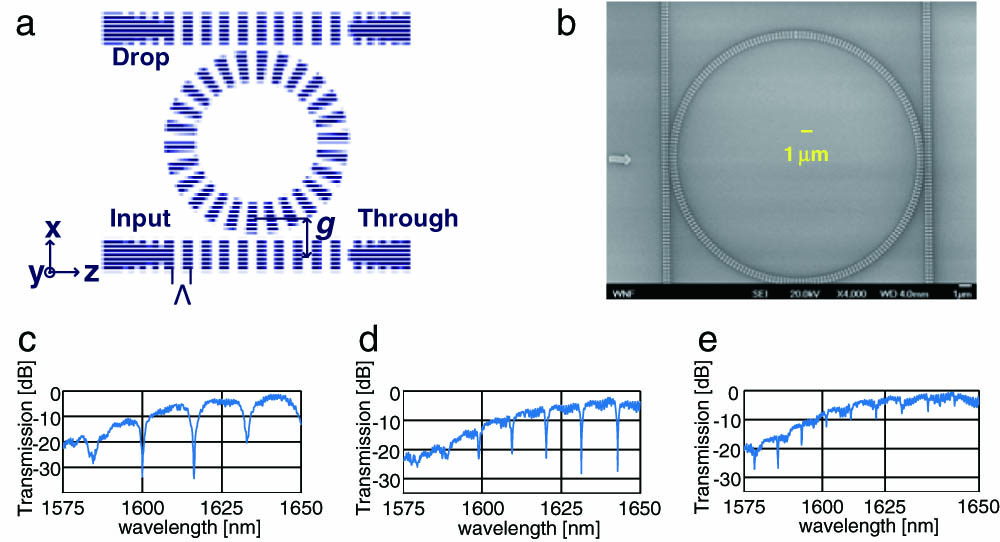
Fig. 2. Conventional MRR based on SWG waveguides in SOI: (a) schematic and (b) SEM prior to top oxide cladding deposition, and measured through responses (normalized) for a ring radius of (c) 15, (d) 20, and (c) 25 μm.

下载图片 查看所有图片

Due to the longer coupling region between the resonator and bus waveguides, racetrack designs may be preferred. Figure 3 shows the layout and a zoom of a racetrack resonator based on SWG waveguides. The length of the directional coupling section L along with the gap g determine the coupling efficiency and operating condition (under-coupled, critically coupled, or over-coupled) of the resonator. The curved section has a radius r, and the total perimeter of the racetrack that determines the free spectral range (FSR) is 2πr+2L. For an experimental implementation, we considered the same SWG waveguide parameters as for the MRRs as well as r=20μm, L=40μm, and g=600nm. Figure 3(c) shows the measured through and drop responses; the fiber-to-fiber loss is also 16dB. An extinction ratio as high as 33 dB was obtained at a wavelength of 1527.9 nm; the corresponding Q-factor is 1530. On the other hand, the limited extinction ratio in the drop response may be due to the directional coupling/operating condition.
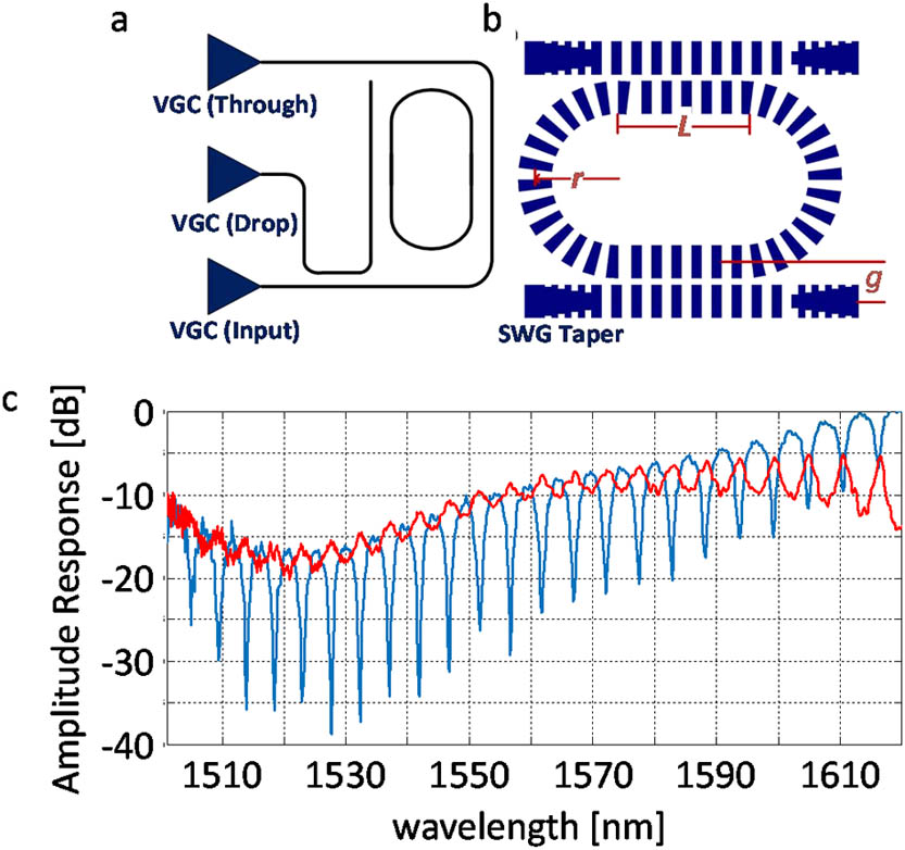
Fig. 3. SWG racetrack resonator: (a) layout, (b) detailed view, and (c) measured through (blue) and drop (red) responses (normalized). See text for device parameters.

下载图片 查看所有图片

For some filtering applications, the periodic nature of MRRs is undesirable. In this context, BGs are more suitable. BGs can be realized by inducing periodic variations in the refractive index along the direction of propagation as well as physical corrugations or variations in the waveguide geometry. We can create a periodic variation in the effective index along the direction of propagation by “interleaving” two SWG waveguides having different duty cycles. Figure 4(a) shows the schematic of such an SWG BG, in which two SWG waveguides with duty cycles D1=(a1/Λ1) and D2=(a2/Λ2) are interleaved; the period of the SWG BG is Λ1+Λ2. We fabricated an SWG BG based on waveguides with a cross-section h=220nm×W=500nm and periods Λ1=Λ2=280nm. The SWG BG has 2000 periods, for a total length of 1.12 mm. To extract the reflection response, we use a compact Y-branch based on conventional silicon nanowire waveguides. We also use the same SWG taper and VGC designs as for the MRRs. The VGCs are separated by 127 μm, and a fiber ribbon array is used for testing. The device occupies a footprint of 1.18mm×254μm. Figures 4(b) and 4(c) show the device layout and an SEM image of an SWG BG prior to the deposition of the top oxide, respectively.
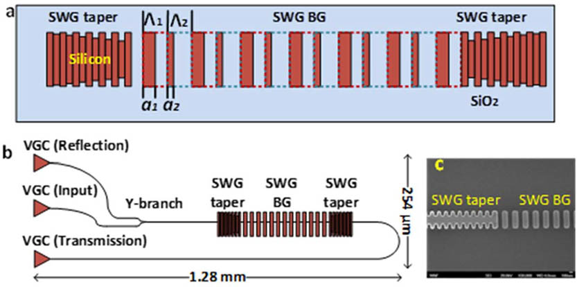
Fig. 4. SWG BG: (a) schematic of SWG BG formed by interleaving two SWG waveguides of different duty cycles, (b) device layout for experimental demonstration, and (c) SEM of the fabricated SWG BG prior to the oxide cladding deposition.

下载图片 查看所有图片

Figure 5 compares the transmission response of an SWG BG with D1=50% and D2=48% with that of a simple SWG waveguide. The SWG BG exhibits a clear rejection peak at a resonant wavelength of 1546.8 nm and the transmission loss is 12dB, corresponding to a peak reflectivity of 90.4%. The 3 dB bandwidth is 0.5 nm and the total fiber-to-fiber loss 15dB.

Fig. 5. (a) Measured transmission spectrum of SWG BG and simple SWG waveguide (see text for parameters). The difference in transmission responses is due in part to the spectral response of the Y-branch (optimized for 1550nm), which is present in the SWG BG only. (b) Zoom of the transmission (blue) and reflection (green) responses about the resonant peak at 1546.8 nm.

下载图片 查看所有图片

One drawback of two-port BG devices is that they typically operate in reflection, which usually translates into the need for optical circulators or a Y-branch (splitter/coupler), which, in turn, induces additional optical loss and can impact the gain in an MWP system. On the other hand, wideband BG-defined filtering requirements can be obtained using compact SOI grating-assisted CDCs, which are intrinsically four-port (add–drop) devices[18]. Grating-assisted CDCs are based on two closely spaced (and asymmetric) waveguides and some form of periodic refractive index perturbation along the waveguides. We demonstrate an alternate approach whereby the asymmetric waveguides and grating mechanism are replaced by an SWG waveguide in proximity to a continuous waveguide. In SOI, because of the large optical phase mismatch between the SWG and nanowire waveguides, undesired codirectional coupling can be efficiently suppressed. Moreover, the SWG waveguide provides the required grating mechanism and enables contradirectional coupling. The strong index variation in the SWG leads to a relatively strong coupling coefficient such that power transfers can be obtained using relatively short coupling lengths.

The schematic of the proposed design and the layout of a fabricated device are illustrated in Figs. 6(a) and 6(b). A conventional nanowire waveguide is gradually brought to a gap distance g from an SWG waveguide to create the coupler waist having length LC. As before, the cross-section of the SWG and nanowire waveguides is h=220nm×W=500nm; the SWG has a period Λ=378nm and D=50%. The SWG tapers have P=250nm and a width variation from 500 nm down to 150 nm over a length of 15 μm, and input/output coupling is performed with VGCs. Figure 6(c) shows the measured through and drop responses for an SWG CDC with LC=400μm and g=150. The bandwidth of the drop/through responses is 16nm and the extinction ratio is >35dB. Due to the large degree of asymmetry in the effective refractive indices of the SWG and conventional nanowire waveguides, there is a large wavelength separation between the resonant (drop) wavelength of the SWG CDC at λC and unwanted intra-waveguide back reflections (at λR1 and λR2). Figure 6(d) shows the simulated response for an SWG CDC with Λ=378nm, g=200nm, and LC=100μm. There is a single-band operating window of nearly 200 nm, which can exceed that of previously demonstrated grating-assisted CDCs in SOI.
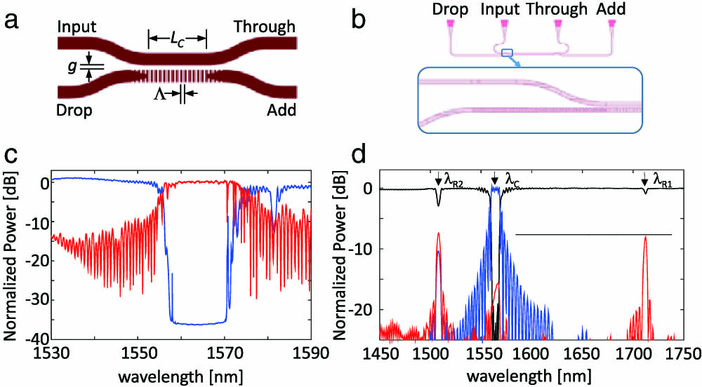
Fig. 6. (a) Schematic of the proposed SWG CDC in SOI, (b) layout of a device with LC=50μm, (c) measured drop (red) and through (blue) responses (see text for device parameters), and (d) 3D FDTD simulated response for SWG CDC with Λ=378nm, g=200nm, and LC=100μm.

下载图片 查看所有图片

The MRRs, BGs, and CDCs are fundamental building blocks that have immediate application in MWP signal processing as well as in implementing more complex devices and systems. For example, due to their wavelength-selective nature, the amplitude response of MRRs and BGs can implement frequency discrimination filters for phase modulation-to-intensity modulation conversion with applications for UWB waveform generation[2]. MRRs can be cascaded to obtain higher-order filter responses or to provide time delays[5]. A serial array of BGs at different resonant wavelengths can also be used to implement a discretely tunable delay line[19]. Cascaded MRRs with different resonant wavelengths (i.e., unique wavelengths within an FSR) or BGs can be used as spectral shapers for generating chirped microwave waveforms based on the principle of spectral shaping followed by wavelength-to-time mapping[7,20,21]. Finally, the spectral response of the CDCs can be tailored by controlling the SWG parameters or coupling parameters. In particular, phase shifts can be applied to realize resonances within the drop response. Such equivalent “phase-shifted” grating responses have applications for performing temporal operations such as differentiation and Hilbert transformation[2224" target="_self" style="display: inline;">–24]. It has been shown that SWG waveguide crossings exhibit low loss (0.023dB/crossing) and crosstalk (<40dB)[25]. Thus, one advantage of implementing building blocks based on SWG waveguides is the potential for very dense integration.

A number of techniques exist to implement an optical delay passively, i.e., without gain, and broadly speaking, these can be divided in two categories: (1) length-variable delay lines whereby the propagation length (L) of the delay element is varied (i.e., the delay Δt is given by L/vg where vg is the propagation group velocity) and (2) variable propagation velocity delay lines where vg is varied (for some implementations, this is also known as a wavelength-variable delay line). These two approaches encompass employing a fixed length of waveguide, fiber, or free space as the delay medium, as well as resonance enhancements in which the physical path of the delay medium is enhanced through a cavity or by exploiting resonances where dispersion can be large. There is a well-established trade-off between the amount of resonance enhancement that can be obtained (and hence the amount of optical delay) and the operating bandwidth. As such, in this paper, we consider only optical delay lines (ODLs) that do not involve resonance enhancements.

An ODL that provides time delays for pulses or signals at the same optical carrier is one form of an OTTDL. The conventional architecture of such an OTTDL employs an array of waveguides of different lengths whereby the difference in lengths induces the differential/incremental delay between waveguides (also referred to as taps). For discrete tuning, the different lengths of waveguides can be cascaded using switches or splitters/combiners. To reduce the chip size for integrated implementations, the waveguides are typically arranged with spiral or curvy/serpentine topologies. Indeed, impressive results of 4-bit and 7-bit delays have been obtained in SOI and silicon nitride[26,27].

To minimize or reduce complexities associated with length-variable OTTDLs is to develop an index-variable OTTDL, where true time delay control can be obtained through variation in the group index or propagation velocity in the waveguides. Gasulla and Capmany proposed to exploit the parallelism inherent in multicore fibers to implement an index-variable OTTDL, where the true time delay of each tap can be controlled through designing a proper physical dimension and material doping concentration of each fiber core[28].

The use of SWG waveguides to create a delay or path mismatch in a Mach–Zehnder interferometer was demonstrated recently[29]. We built on this idea and took advantage of the ability to tune the effective index of an SWG waveguide through control of its duty cycle D to realize an integrated index variable OTTDL[30].

To investigate the minimum incremental time delay that is possible, we fabricated 2-arm MZIs incorporating SWG waveguides with different duty cycles in each arm, i.e., with a duty cycle difference of ΔD, as shown in Fig. 7(a). The SWG waveguides in each arm have the same length of 8 mm. The SWG waveguides have a cross-section of h=220nm×W=500nm and a period Λ=250nm. The SWG waveguides are coupled to conventional silicon nanowires (used for the Y-branches) with the same taper designs as for the SWG MRRs and BGs. Figure 7(b) shows the measured spectral responses; the FSRs are 5, 2.9, and 1.7nm for ΔD=1%, 2%, and 3%, respectively, corresponding to delay differences of 1.6, 2.8, and 4.7 ps between the MZI arms. The minimum achievable time delay will scale proportionally with the length of the SWG waveguide, and sub-picosecond time delay resolutions can be expected with shorter waveguides (<8mm).
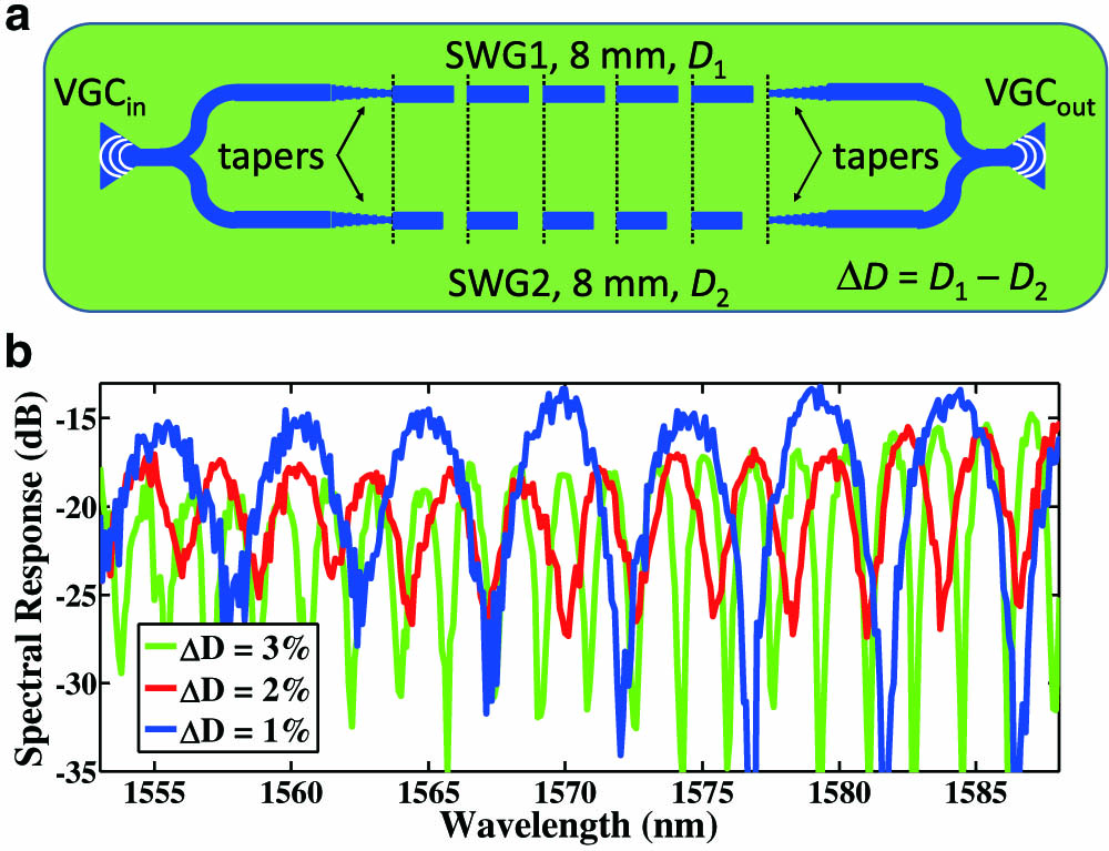
Fig. 7. (a) Schematic of MZI incorporating SWG waveguides with different duty cycles D1 and D2 in each arm. (b) Measured spectral responses of MZIs with ΔD=1%, 2%, and 3%.

下载图片 查看所有图片

Next, we fabricated an OTTDL for microwave phase shifting. The structure comprises an array of 4 separate SWG waveguides (a microwave signal modulated on an optical carrier will experience a different phase shift when propagating through the different SWG waveguides) of the same length (8 mm) and where the duty cycles are varied in 10% increments from D1=60% to D4=30%; a reference path comprising a short length of nanowire waveguide that connects the input and output VGCs is also included, see Fig. 8(a). The SWG waveguides are separated by 127.5 μm, and the OTTDL occupies a chip size of 0.51mm×8.06mm. The SWG waveguides have the same parameters as for the 2-arm MZIs.

The measured RF phase shift as a function of the frequency from the 4 different SWG waveguides is shown in Fig. 8(b). The time delay of each waveguide can be estimated from the average slope of the measured phase shift vs. the frequency response. The incremental time delays are 8.9, 10.7, and 7.9 ps between the SWG waveguides, with D1=60%, D2=50%, D3=40%, and D4=30%. Note that while the duty cycles of the SWG waveguides are varied in increments of 10%, this does not translate into a linear change in the incremental time delay, as the group index of the SWG waveguide is not a linear function of the duty cycle.
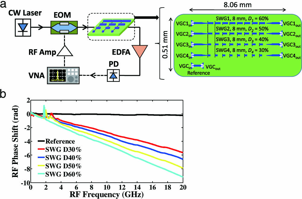
Fig. 8. (a) Schematic of OTTDL based on an array of 4 SWG waveguides and experimental setup for microwave phase shift measurements. (b) Measured RF phase shift vs. modulation frequency for an optical carrier at 1565 nm.

下载图片 查看所有图片

We have provided an overview of the recent work on developing wavelength-selective SWG waveguide filters based on MRRs, BGs, and CDCs, as well as index-variable OTTDLs. Since SWG waveguides are based on the same technology and waveguide design as silicon nanowires, they are compatible with existing silicon photonic devices, e.g., switches and modulators. As such, SWG waveguides enhance the available component toolbox for developing integrated MWP systems in SOI. The technological developments described here, along with others in silicon photonics, point to the feasibility of more complex integrated MWP systems that can provide increased functionality and, ultimately, performance.

References

[1] CapmanyJ.NovakD., Nat. Photon.1, 319 (2007).NPAHBY1749-4885

[2] YaoJ., IEEE/OSA J. Lightwave Technol.27, 314 (2009).

[3] IezekielS.BurlaM.KlamkinJ.MarpaungD.CapmanyJ., IEEE Microwave Mag.16, 28 (2015).1527-3342

[4] MarpaungD.RoeloffzenC.HeidemanR.LeinseA.SalesS.CapmanyJ., Lasers Photon. Rev.7, 506 (2013).

[5] RoeloffzenC. G. H.ZhuangL.TaddeiC.LeinseA.HeidemanR. G.van DijkP. W. L.OldenbeuvingR. M.MarpaungD. A. I.BurlaM.BollerK.-J., Opt. Express21, 22937 (2013).OPEXFF1094-4087

[6] MarpaungD.PaganiM.MorrisonB.EggletonB. J., IEEE/OSA J. Lightwave Technol.32, 3421 (2014).

[7] ZhangW.YaoJ., IEEE J. Quantum Electron.52, 0600412 (2016).IEJQA70018-9197

[8] BockP. J.ChebenP.SchmidJ. H.LapointeJ.DelâgeA.JanzS.AersG. C.XuD.-X.DensmoreA.HallT. J., Opt. Express18, 20251 (2010).OPEXFF1094-4087

[9] ChenandX.TsangH. K., Opt. Lett.36, 796 (2011).OPLEDP0146-9592

[10] XuX.SubbaramanH.CoveyJ.KwongD.HosseiniA.ChenR. T., Appl. Phys. Lett.101, 031109 (2012).APPLAB0003-6951

[11] HalirR.Ortega-MoñuxA.SchmidJ. H.Alonso-RamosC.LapointeJ.XuD.-X.Wangüemert-PérezJ. G.Molina-FernándezI.JanzS., IEEE J. Sel. Top. Quantum Electron.20, 279 (2014).IJSQEN1077-260X

[12] DonzellaV.SherwaliA.FlueckigerJ.FardS. T.GristS. M.ChrostowskiL., Opt. Express22, 21037 (2014).OPEXFF1094-4087

[13] HalirR.BockP. J.ChebenP.Ortega-MoñuxA.Alonso-RamosC.SchmidJ. H.LapointeJ.XuD.-X.Wangüemert-PérezJ. G.Molina-FernándezÍ.JanzS., Lasers Photon. Rev.9, 25 (2015).

[14] DonzellaV.SherwaliA.FlueckigerJ.GristS. M.FardS. T.ChrostowskiL., Opt. Express23, 4791 (2015).OPEXFF1094-4087

[15] FlueckigerJ.SchmidtS.DonzellaV.SherwaliA.RatnerD. M.ChrostowskiL.CheungK. C., Opt. Express24, 15672 (2016).OPEXFF1094-4087

[16] WangZ.XuX.FanD.WangY.SubbaramanH.ChenR. T., Sci. Rep.6, 24106 (2016).SRCEC32045-2322

[17] WangJ.GleskI.ChenL. R., Sci. Bull.61, 879 (2016).

[18] ShiW.WangX.LinC.YunH.LiuY.Baehr-JonesT.HochbergM.JaegerN. A.ChrostowskiL., Opt. Express21, 3633 (2013).OPEXFF1094-4087

[19] ChenL. R.LiJ.SpasojevicM.AdamsR., Opt. Express21, 19624 (2013).OPEXFF1094-4087

[20] YaoJ., Opt. Commun.284, 3723 (2011).OPCOB80030-4018

[21] ChenL. R., Opt. Commun.373, 70 (2016).OPCOB80030-4018

[22] BurlaM.CortésL. R.LiM.WangX.ChrostowskiL.AzañaJ., Opt. Express21, 25120 (2013).OPEXFF1094-4087

[23] BurlaM.CortésL. R.LiM.WangX.ChrostowskiL.AzañaJ., Opt. Lett.39, 6181 (2014).OPLEDP0146-9592

[24] BurlaM.LiM.CortésL. R.WangX.Fernández-RuizM. R.ChrostowskiL.AzañaJ., Opt. Lett.39, 6241 (2014).OPLEDP0146-9592

[25] BockP. J.ChebenP.SchmidJ. H.LapointeJ.DelâgeA.XuD.-X.JanzS.DensmoreA.HallT. J., Opt. Express18, 16146 (2010).OPEXFF1094-4087

[26] MoreiraR. L.GarciaJ.LiW.BautersJ.BartonJ. S.HeckM. J. R.BowersJ. E.BlumenthalD. J., IEEE Photon. Technol. Lett.25, 1165 (2013).IPTLEL1041-1135

[27] XieJ.ZhouL.LiZ.WangJ.ChenJ., Opt. Express22, 22707 (2014).OPEXFF1094-4087

[28] GasullaI.CapmanyJ., IEEE Photon. J.4, 877 (2012).

[29] GleskI.BockP. J.ChebenP.SchmidJ. H.LapointeJ.JanzS., Opt. Express19, 14031 (2011).OPEXFF1094-4087

[30] WangJ.AshrafiR.AdamsR.GleskI.GasullaI.CapmanyJ.ChenL. R., Sci. Rep.6, 30235 (2016).SRCEC32045-2322

Lawrence R. Chen. Subwavelength grating waveguide devices in silicon-on-insulators for integrated microwave photonics (Invited Paper)[J]. Chinese Optics Letters, 2017, 15(1): 010004.

引用该论文: TXT   |   EndNote

相关论文

加载中...

关于本站 Cookie 的使用提示

中国光学期刊网使用基于 cookie 的技术来更好地为您提供各项服务,点击此处了解我们的隐私策略。 如您需继续使用本网站,请您授权我们使用本地 cookie 来保存部分信息。
全站搜索
您最值得信赖的光电行业旗舰网络服务平台!