激光与光电子学进展, 2020, 57 (11): 111416, 网络出版: 2020-06-02
飞秒激光空间光束整形加工技术研究进展  下载: 2266次特邀综述
Progress in Femtosecond Laser Processing Technology Based on Space Beam Shaping
图 & 表
图 1. 多焦点并行加工微透镜阵列电镜图(SEM)[1]。(a)三角形分布微透镜阵列;(b)图(a)以45°观察的局部图像;(c)六边形分布微透镜阵列;(d) 4×4微透镜阵列
Fig. 1. SEM images of microlens arrays fabricated by multiple foci[1]. (a) Microlens arrays in triangle distribution; (b) partial view of one microlens in Fig. (a) captured at 45°; (c) microlens arrays in hexagonal distribution; (d) microlens arrays in 4×4 distribution
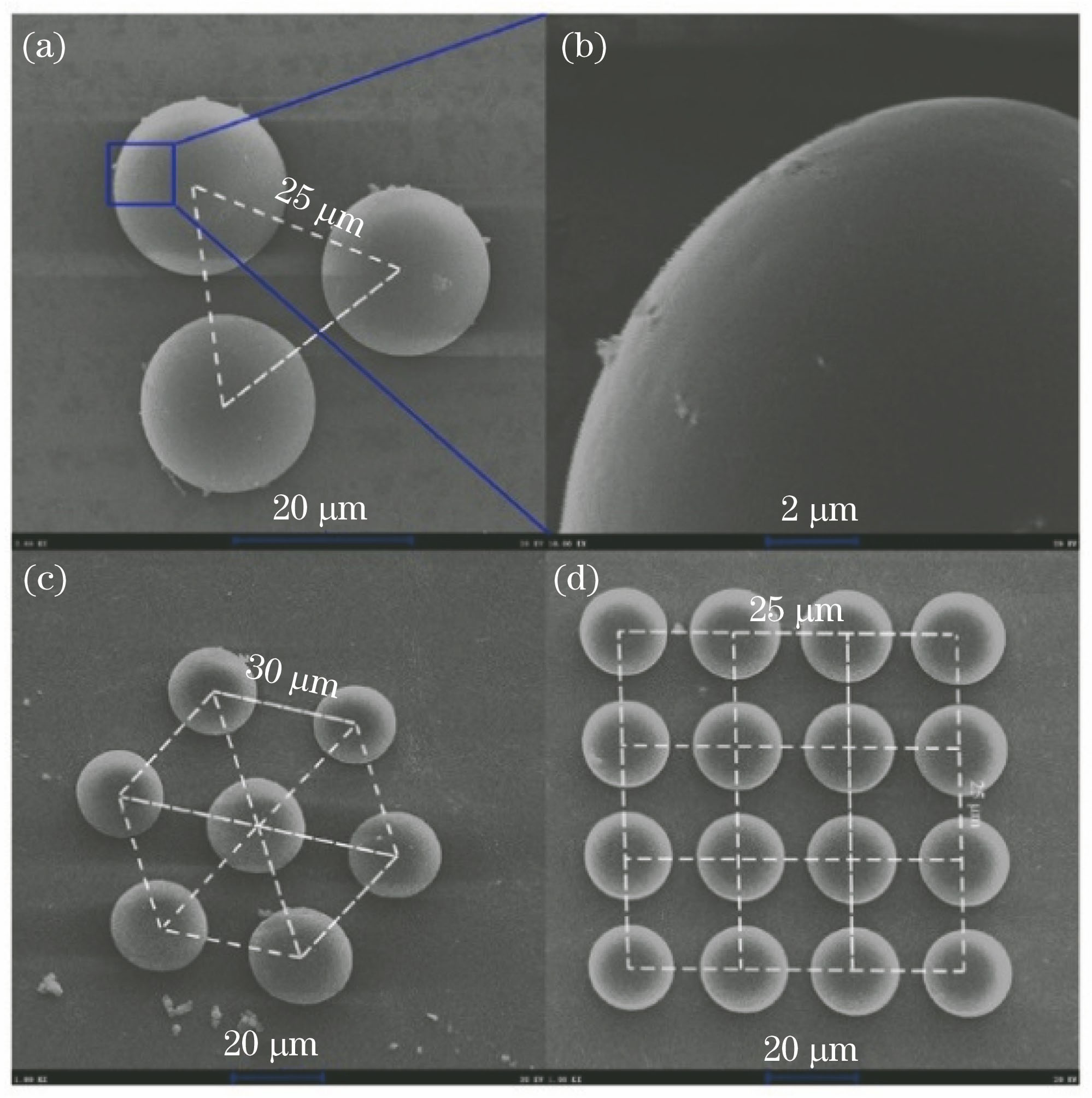
图 2. 多焦点在微通道内部集成不同微过滤器及过滤器微孔尺寸与激光能量的关系[3]。(a)(b)五焦点和七焦点集成微过滤器示意图;(c)(d)五焦点和七焦点在微通道集成微过滤器电镜图;(e)激光功率与微过滤器孔径的关系
Fig. 2. Multiple foci integration of different microfilters inside the microchannel and dependence of the hole size formed in the filters on the laser power[3]. (a)(b) Schematic illustrations of five foci and seven foci integration of microfilter; (c)(d) SEM images of the microfilters integrated in the microchannel by using five foci and seven foci, respectively; (e) dependence of the hole size formed in the filter on the laser power

图 4. 多光束干涉在单晶硅表面形成的微结构电镜图[7]
Fig. 4. SEM image of microstructure on the surface of silicon by multi beams interference[7]
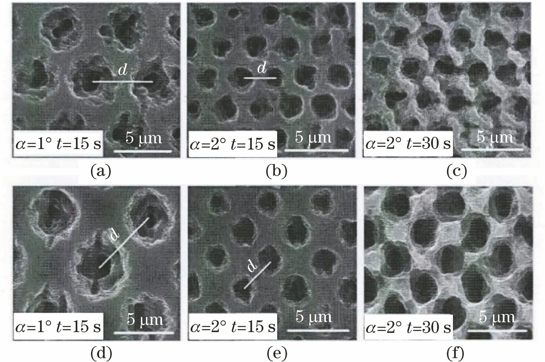
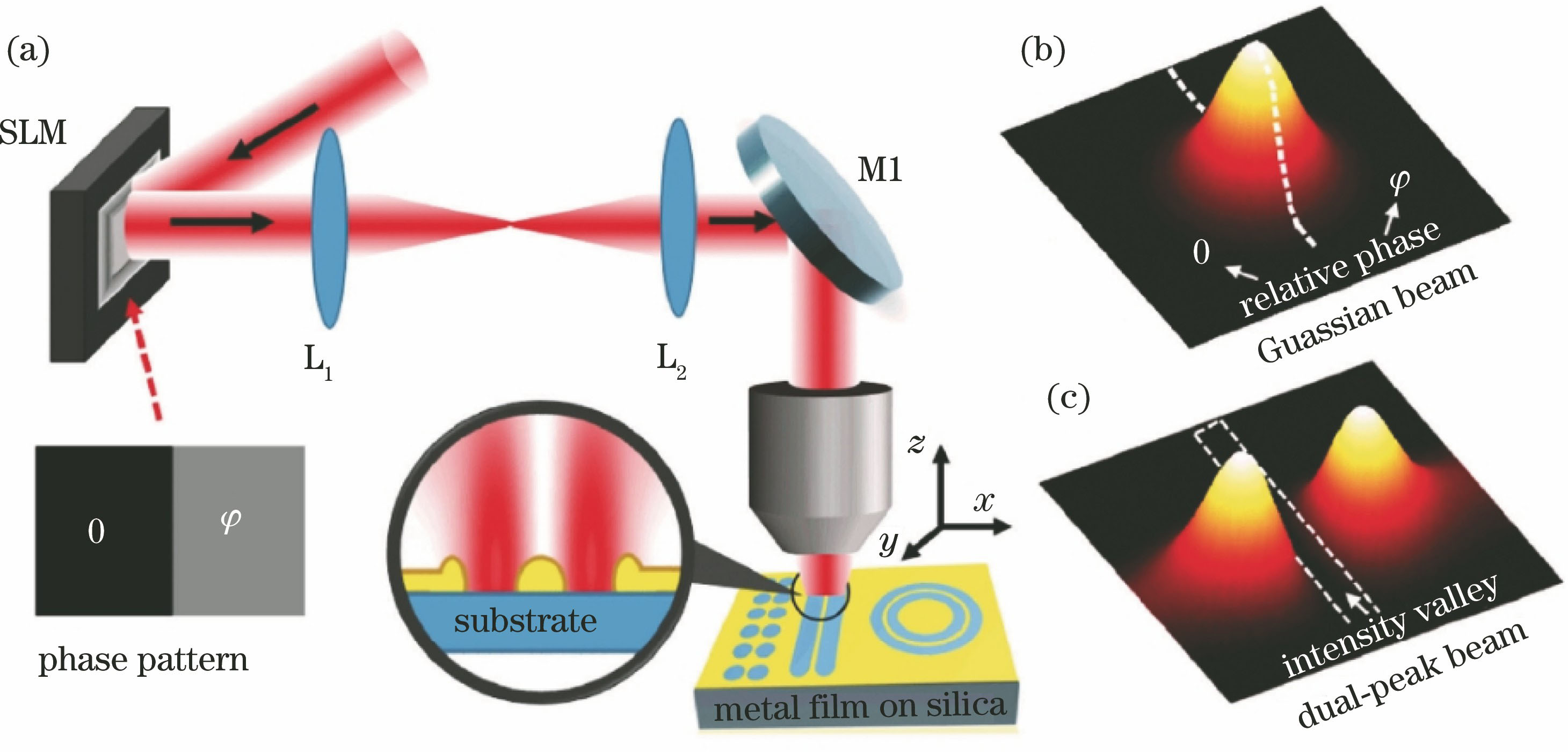
图 6. 实验结果。(a)三光束干涉加工表面结构;(b)四光束干涉加工表面结构[11]
Fig. 6. Experimental results. (a) Surface structures fabricated by three-beam interference; (b) four-beam interference[11]
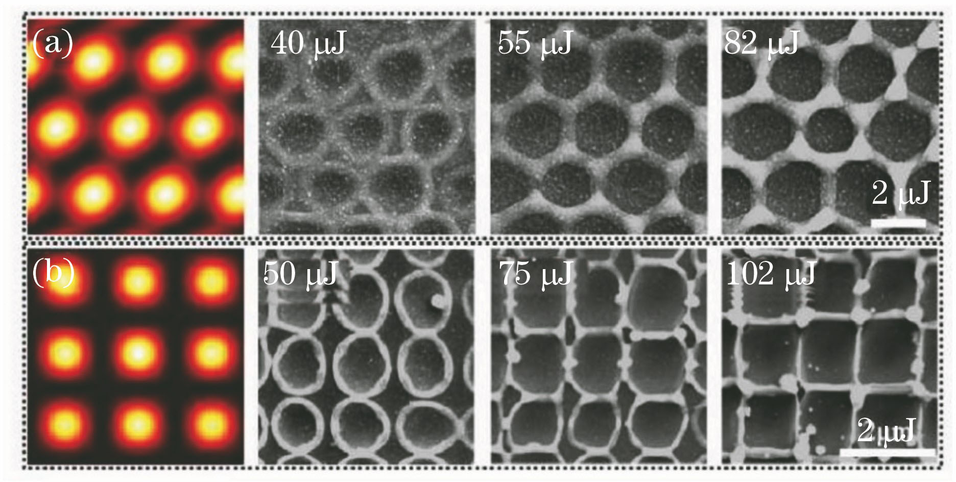

图 10. SLM将飞秒激光调制为圆形/正方形/三角形,应用于双光子光刻[17]
Fig. 10. Femtosecond laser reflected from the SLM was modulated to circle/square/triangular plane and then focused into the photoresist for two-photon polymerization[17]
图 11. 线形光场与抛光示意图[18]。(a)全息柱透镜相位分布;(b)重建光场;(c)线形光场对玻璃表面ITO薄膜进行抛光
Fig. 11. Schematic diagram of line-shape beam and peeling[18]. (a) Phase distribution of holographic cylindrical lens; (b) its optical reconstruction; (c) line-shaped laser peeling of ITO membrane on glass substrate
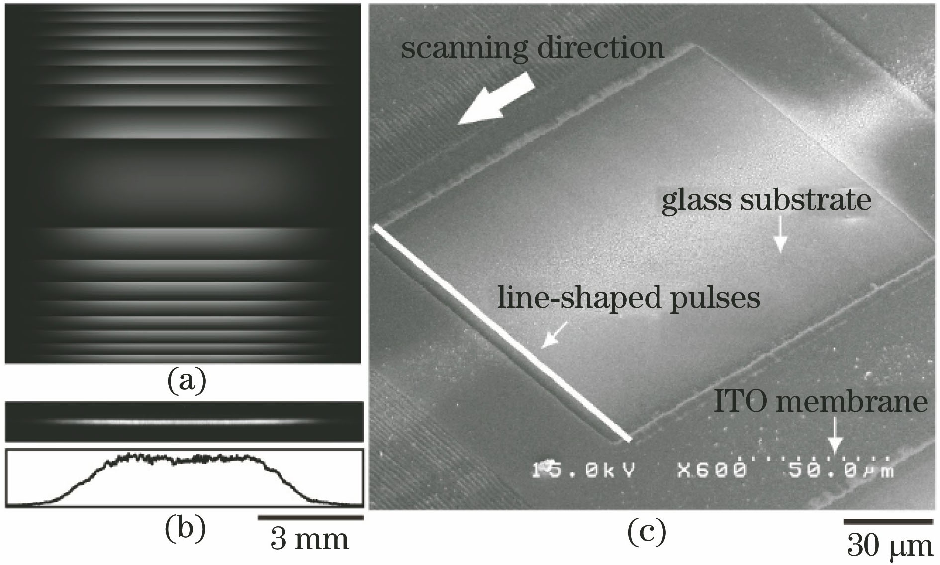
图 12. 利用连续变化光场加工结果的电镜图[19]
Fig. 12. SEM image of processing result with continuous intensity distribution[19]
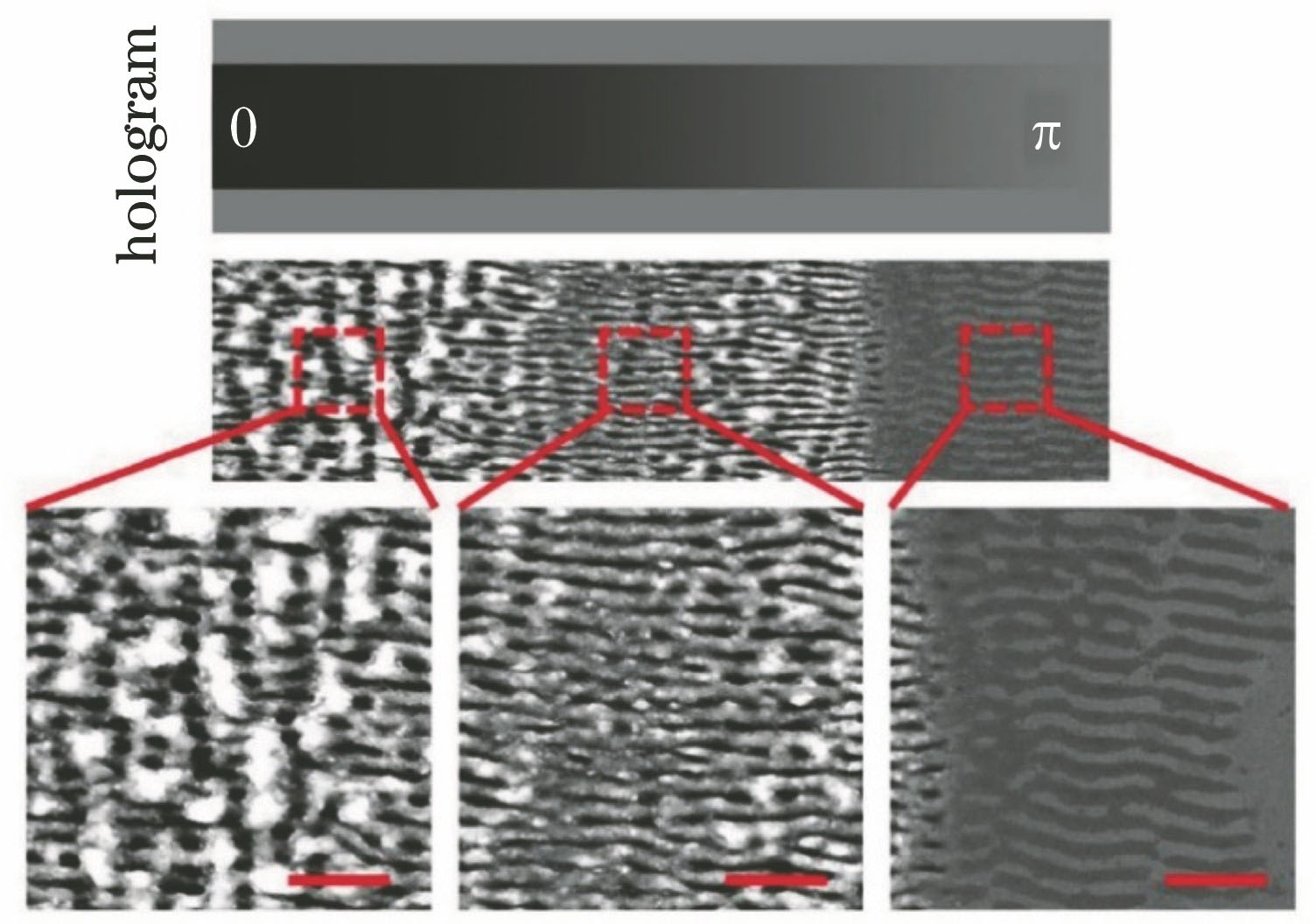
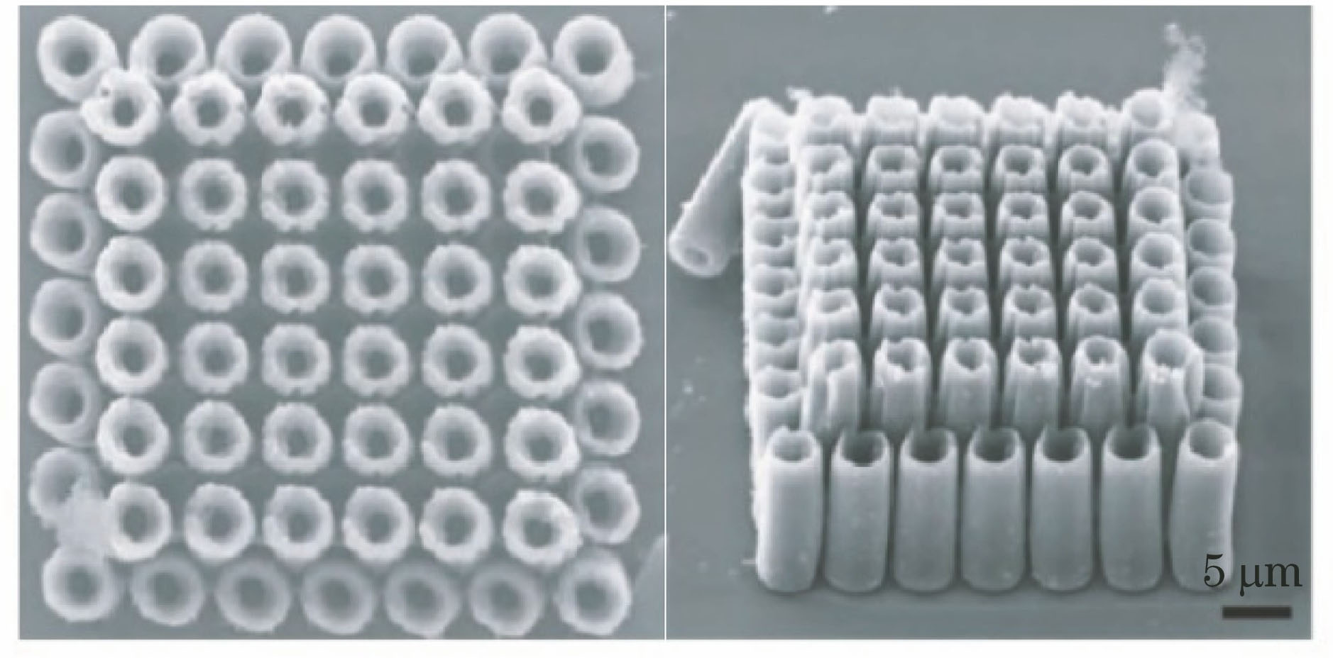
图 14. 利用贝塞尔光束加工3D斜管道和花状微管道阵列[21]
Fig. 14. 3D slant microtubes and flower-like microtube arrays fabricated by tilted the Bessel beam scanning[21]
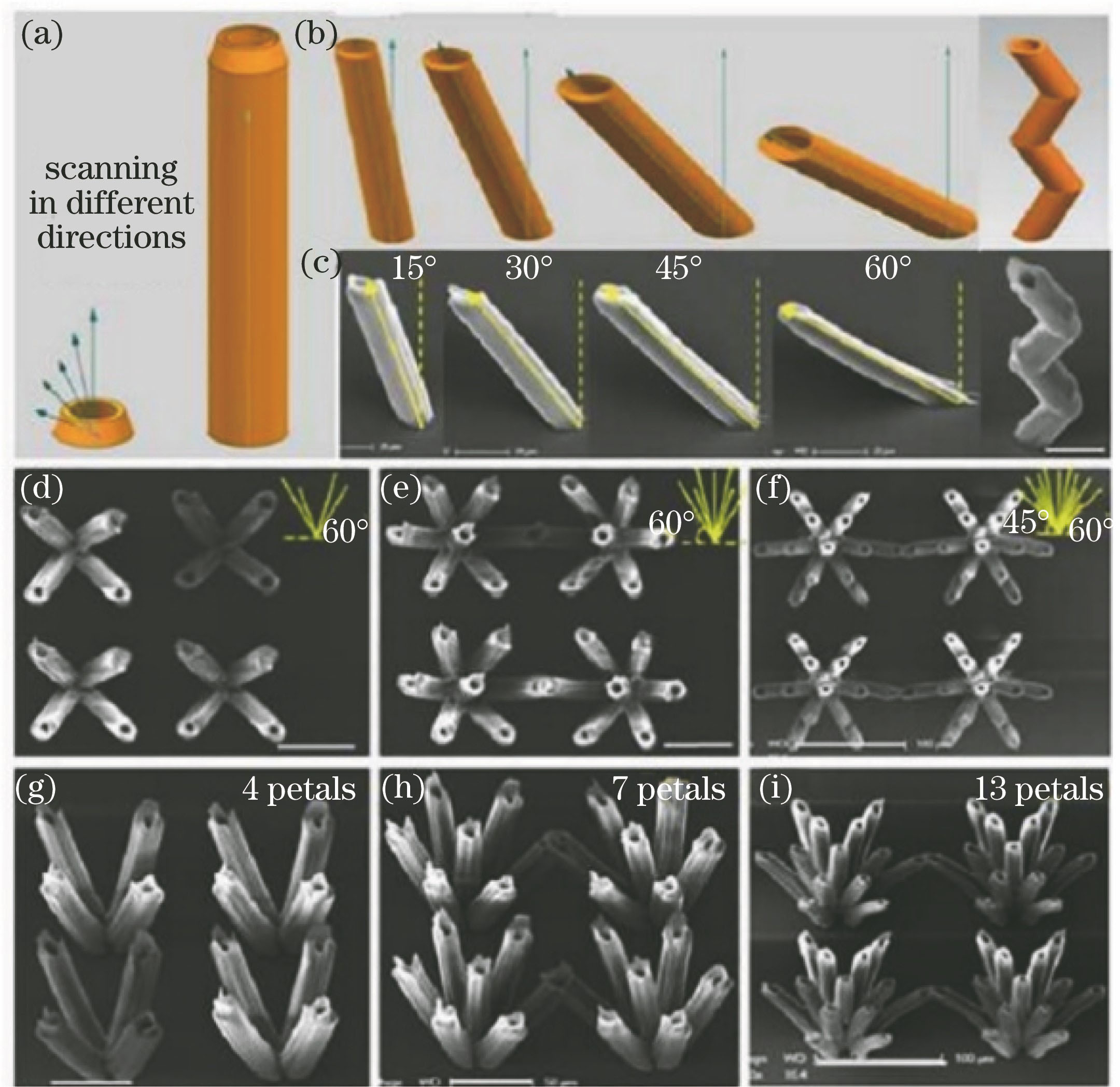
图 15. 动态全息图制造变截面微管道[22]。(a)微管道的类型与拓扑荷和锥透镜半径关系;(b)(c)单环结构外径和内径与锥透镜半径和拓扑荷的关系;(d)微管道加工示意图;(e)直管道电镜图;(f)锥微管道;(g)(h)鼓形微管道
Fig. 15. Dynamic holographic processing of various diameter-varying microtubes[22]. (a) Dependence of different types of microstructures on topological charge and axicon radius; (b)(c) study on the outside diameter and the inside diameter of the single-ring microstructures as a function of axicon radius and topological charge; (d) schematic illustration of the holographic processing of a microtube array; (e) SEM of straight microtube arrays; (f) conical m
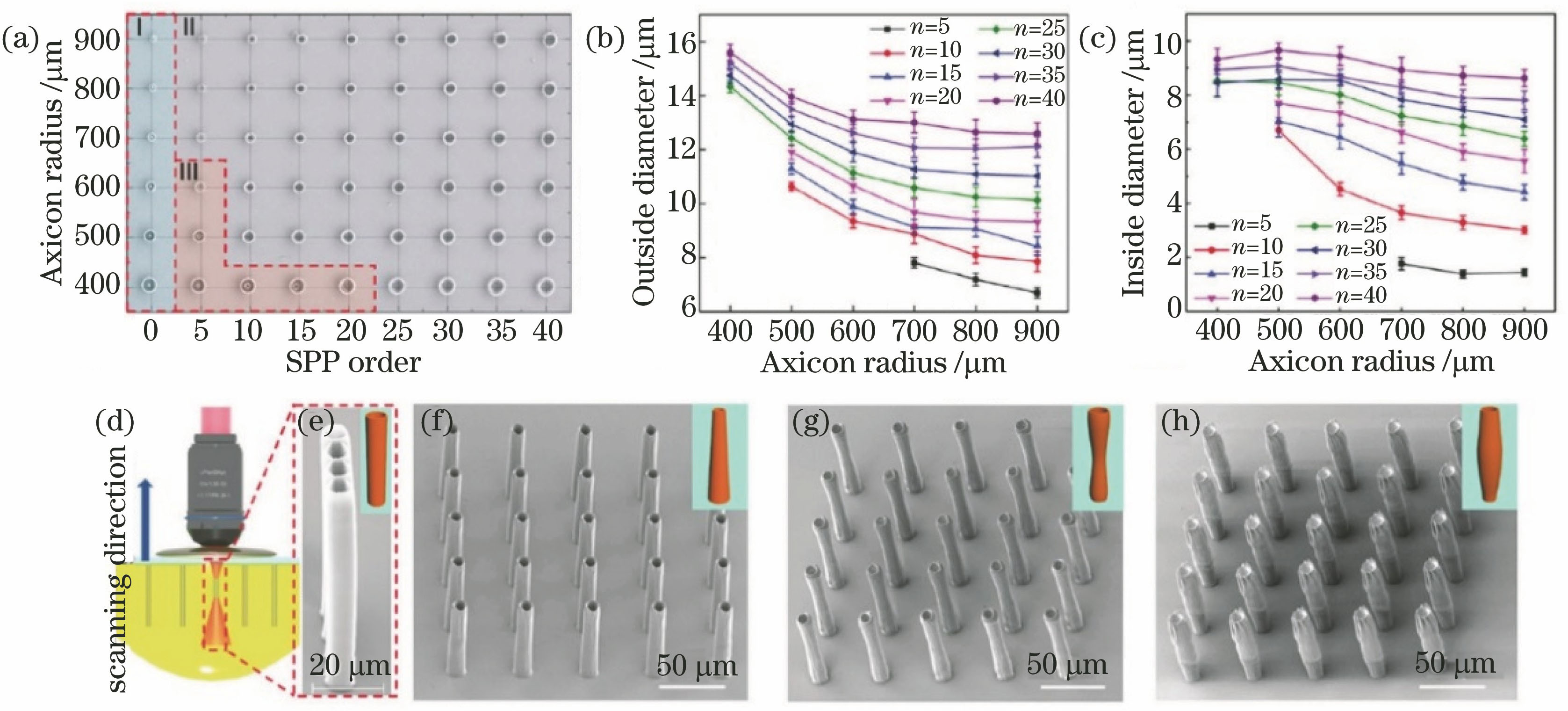
图 16. 缺口环状光场生成方法[23]。(a) SLM加载预设计全息图生成缺口环光束;(b)菲涅耳衍射模拟聚焦光场;(c)计算全息图生成示意图
Fig. 16. Method of creating gap ring shaped light field[23]. (a) Femtosecond gap ring shaped beam is generated by phase modulation using a predesigned hologram loaded in the SLM; (b) simulation of focused light field using Fresnel diffraction; (c) illustration of the computer-generated holograms (CGHs)
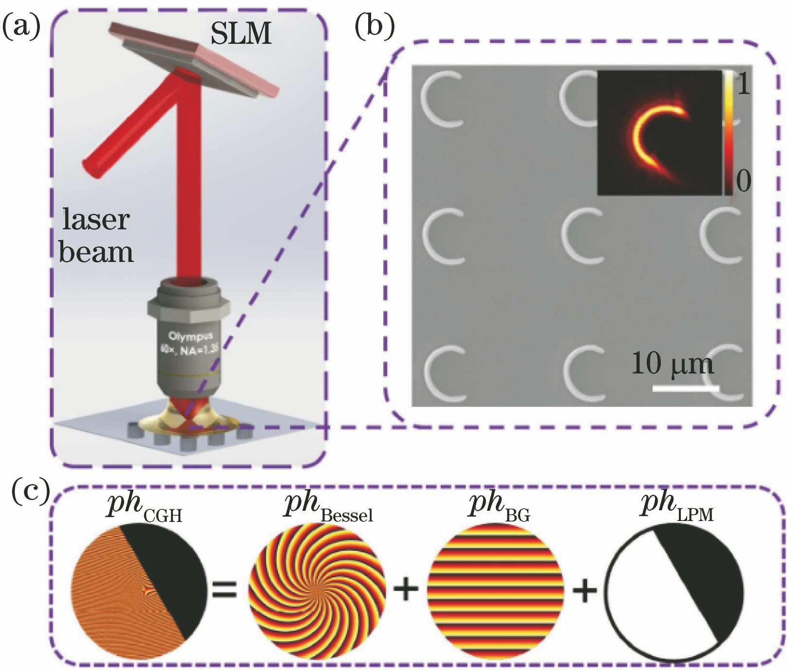
图 17. 由SLM生成的三种光束的相位图,以及在5,10,15,20,25,30 cm处光场强度截面图[25]。(a)贝塞尔光束(2°锥角); (b)准贝塞尔光束, R=+9×10⁵和R=-3×10⁵
Fig. 17. Phase and cross-section intensity profiles at 5, 10, 15, 20, 25, and 30 cm from the SLM for the three types of beams[25]. (a) Bessel beam (2° cone angle); (b) Bessel-like beam, R=+9×10⁵, and R=-3×10⁵
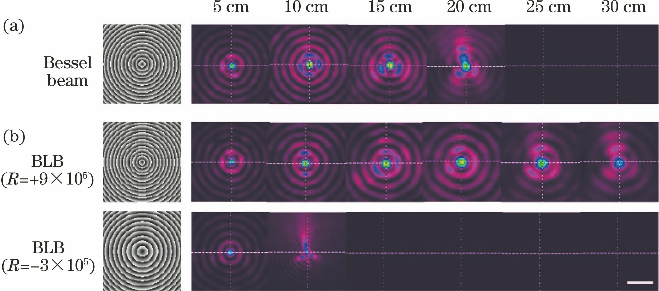
图 18. 零级贝塞尔光束和1+(-1)级叠加贝塞尔光束刻蚀沟槽比较[26]。(a)(c)计算光场形状;(b)(d)对应光束刻划沟槽的原子力显微镜观察图;(e)两种情况下沿扫描方向的光场强度
Fig. 18. Comparison of groove scribing with zero-order and 1+(-1) superposed Bessel beams[26]. (a)(c)Calculated beam shapes; (b)(d) atomic force microscope images of grooves scribed with corresponding beams; (e)comparison of intensities integrated along the scanning direction between two cases
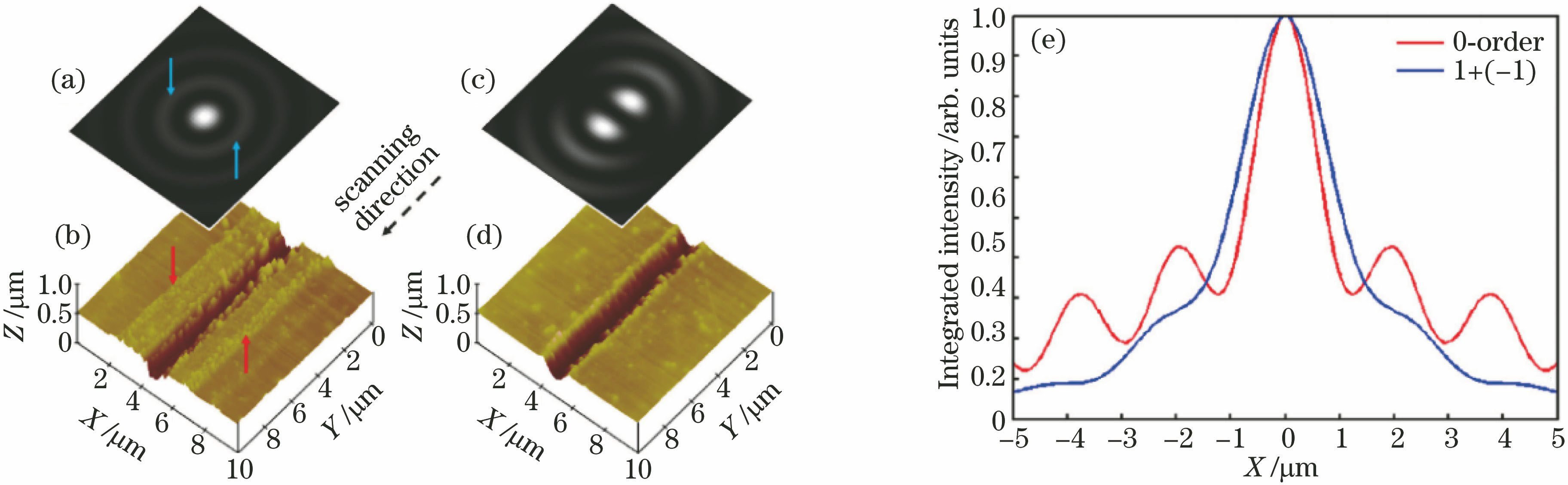
图 19. 利用艾里光束以不同的离焦量加工弯槽结构[27]
Fig. 19. Curved structure were processed by Airy beam with different focuses[27]
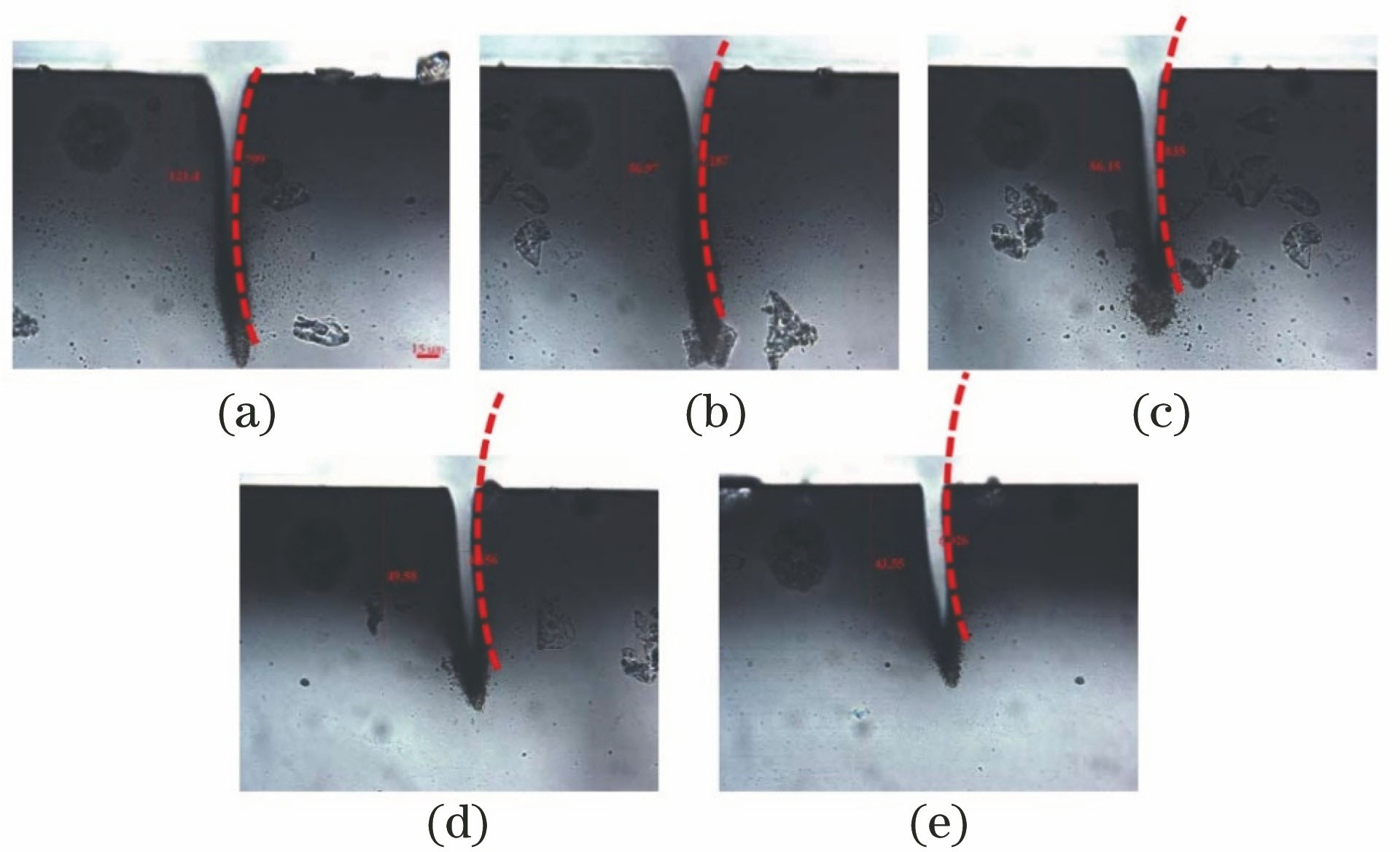
图 20. 利用动态全息加工技术实现多种3D微笼的加工[28]
Fig. 20. Various kinds of 3D microcages fabrication with the dynamic holographic processing technique[28]
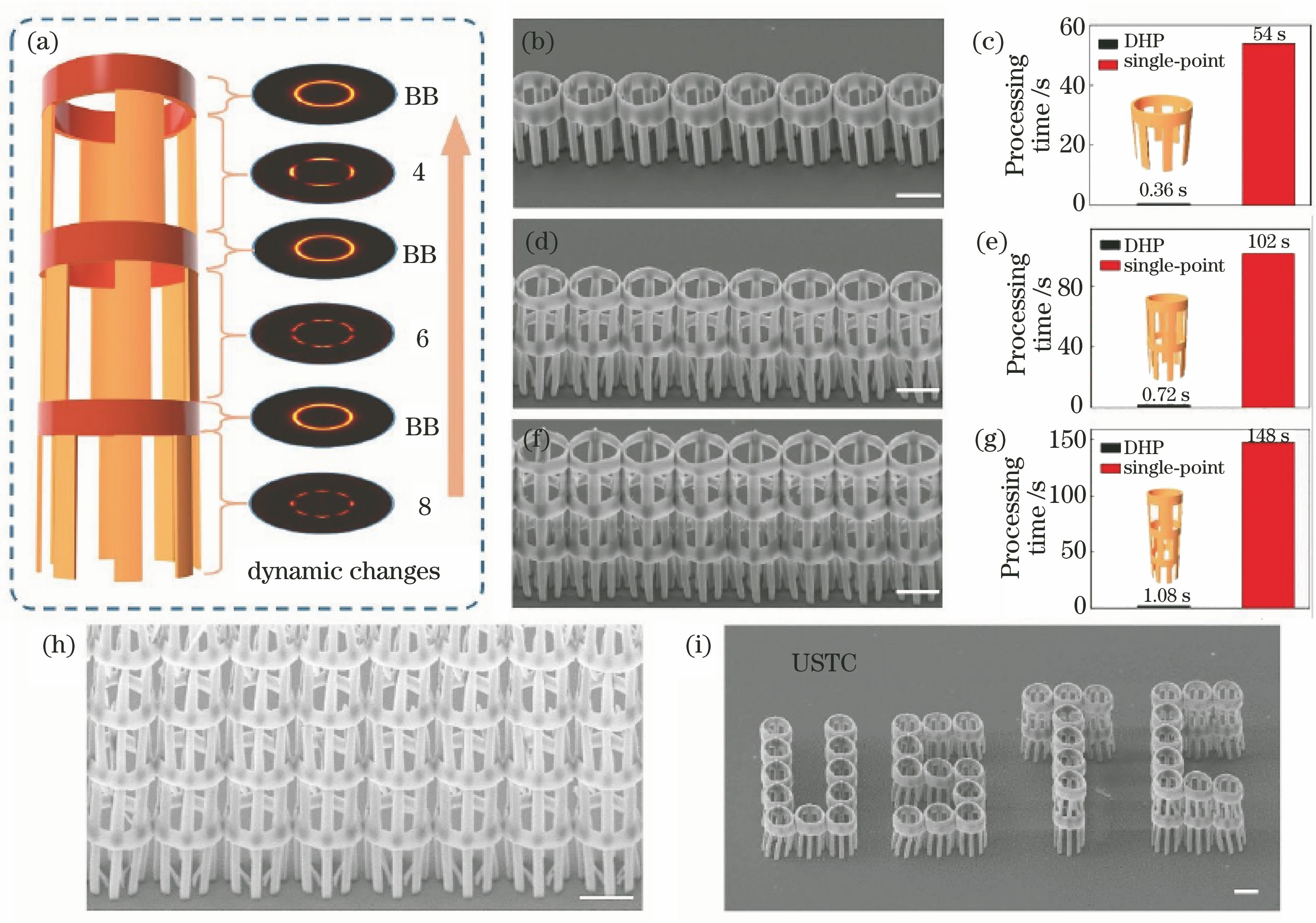
图 21. 聚合制备的双螺旋结构SEM图[31]。(a)双螺旋结构阵列; (b)(c)双螺旋结构的俯视图和侧视图
Fig. 21. SEM images of polymerized double-helix microstructures[31]. (a) Double-helix microstructure array; (b)(c)top and side view of a single double-helix microstructure
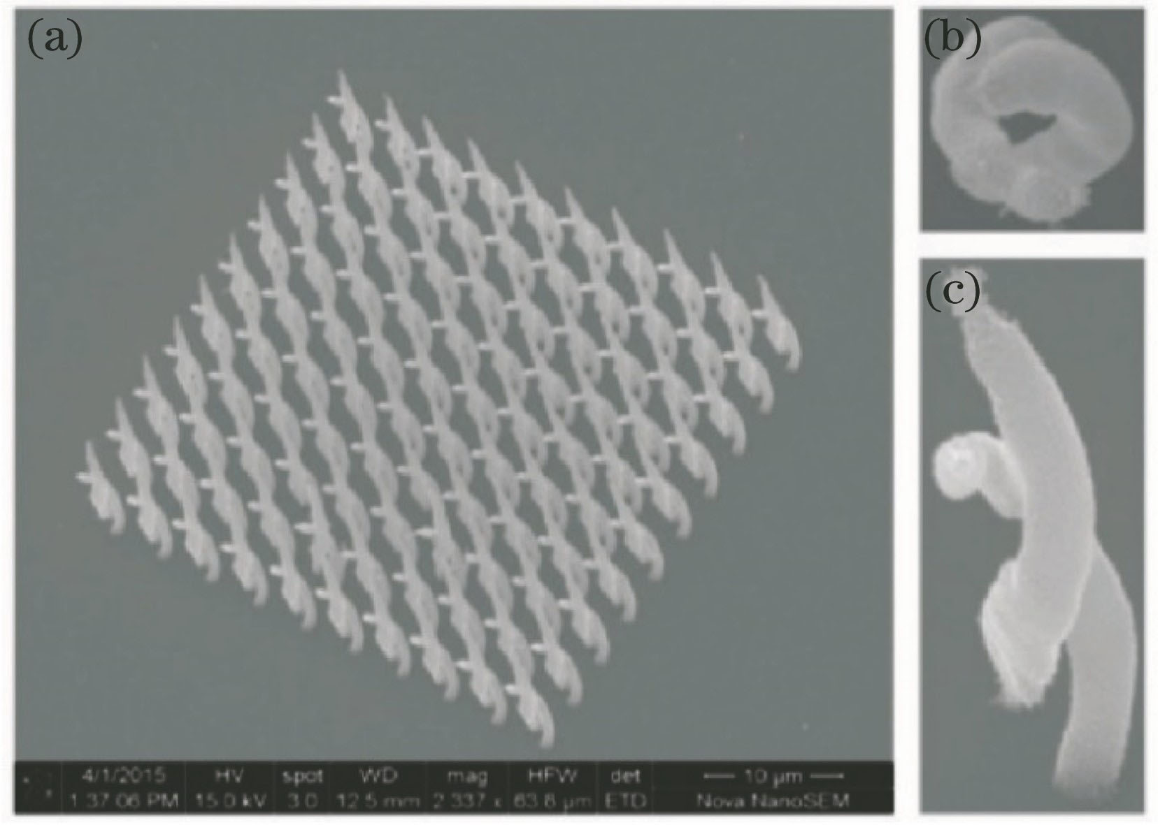
图 22. 利用双螺旋光束还原银双螺旋结构[32]。(a)双螺旋聚焦光场分布;(b)双螺旋阵列的SEM图;(c)测量银双螺旋阵列以常规入射角对左旋圆偏振和右旋圆偏振入射光的透过率
Fig. 22. Photoreduction of silver double helix with double-helix beam[32]. (a) Double-helix focal intensity distribution; (b) SEM images of an array of silver double helix.; (c) measured transmittances of the double-helix silver array for left circular polarization and right circular polarization light at normal incidence
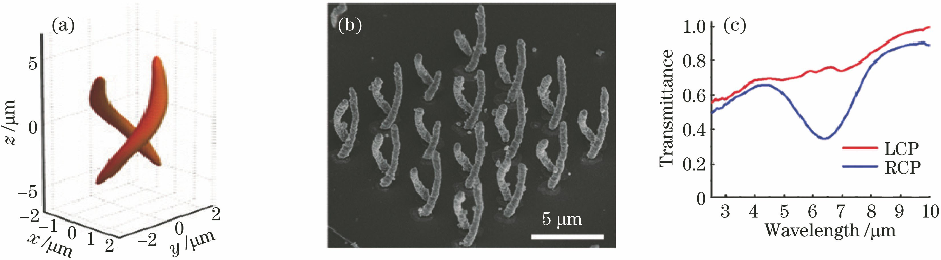
图 23. 线偏振方向在线形光场随位置而发生改变[40]
Fig. 23. Linear polarization directions change with positions in the line-shape beam[40]
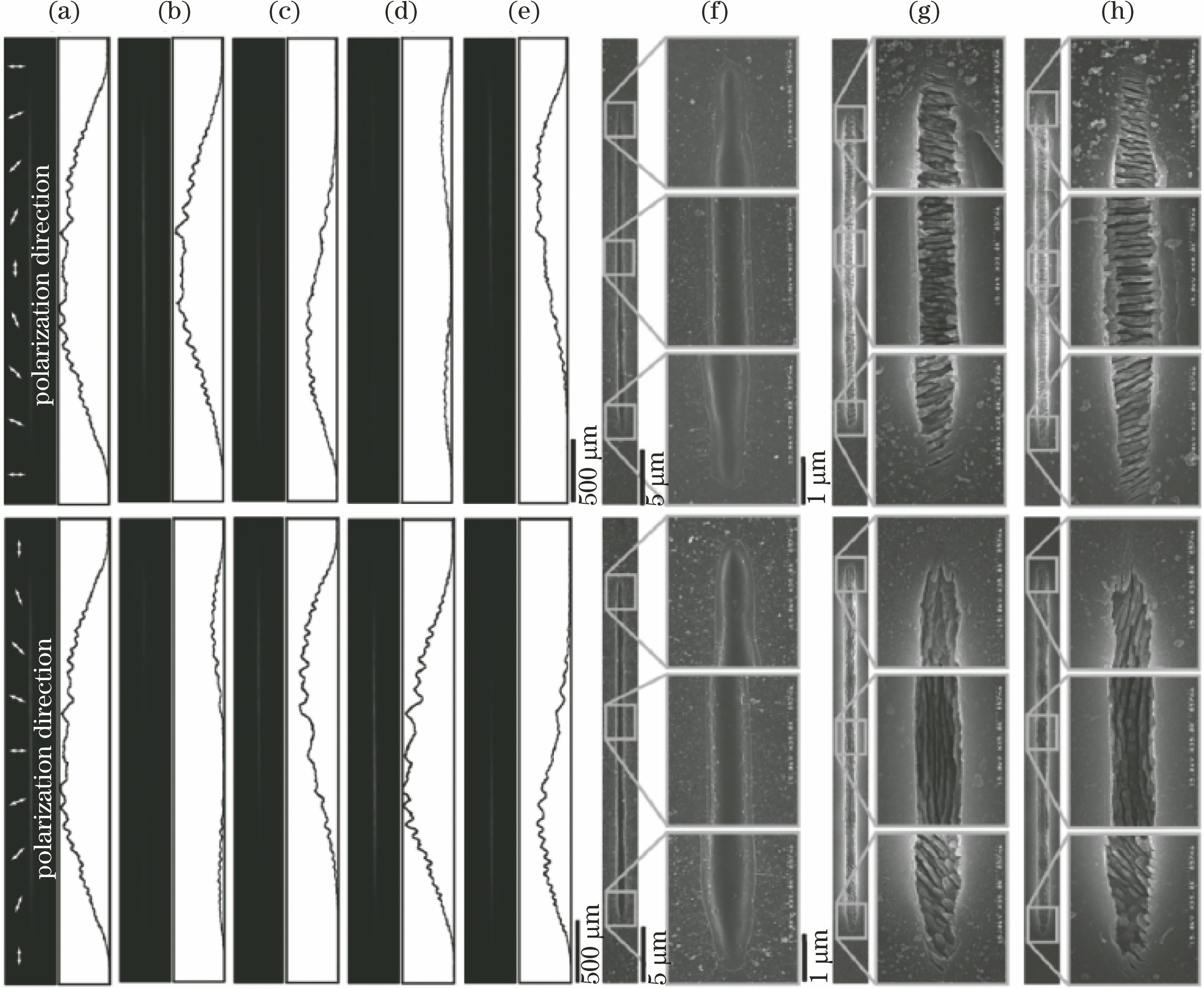
图 24. 圆柱矢量光束的生成[41]。(a)~(c)径向偏振光;(d)~(f)角向偏振光;(g)~(i)风车状偏振光。从左到右依次为调制波前和偏振的全息图、光场重建图、SEM图
Fig. 24. Generations of cylindrical vector beams[41]. (a)-(c) Radial polarization beam; (d)-(f) azimuth polarization beam; (g)-(i) windmill polarization beam. From the left to right, two CGHs for the wavefront and polarization modulations, the optical reconstruction, and the SEM images of fabricated structure
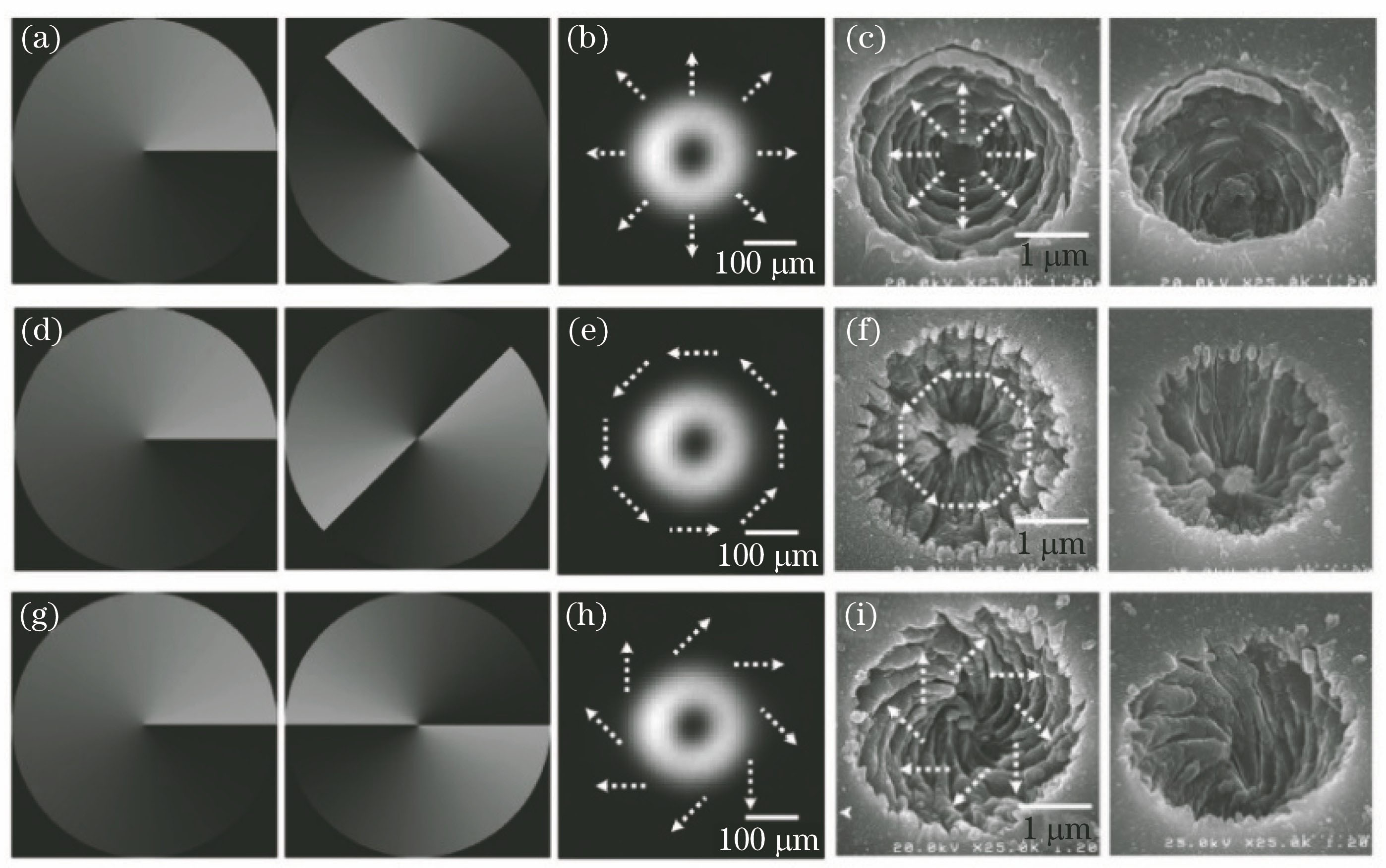
图 25. 不同光栅周期对光场质量和加工形貌的影响[47]
Fig. 25. Effects of different grating cycles on the quality of optical field and the shape of processing[47]
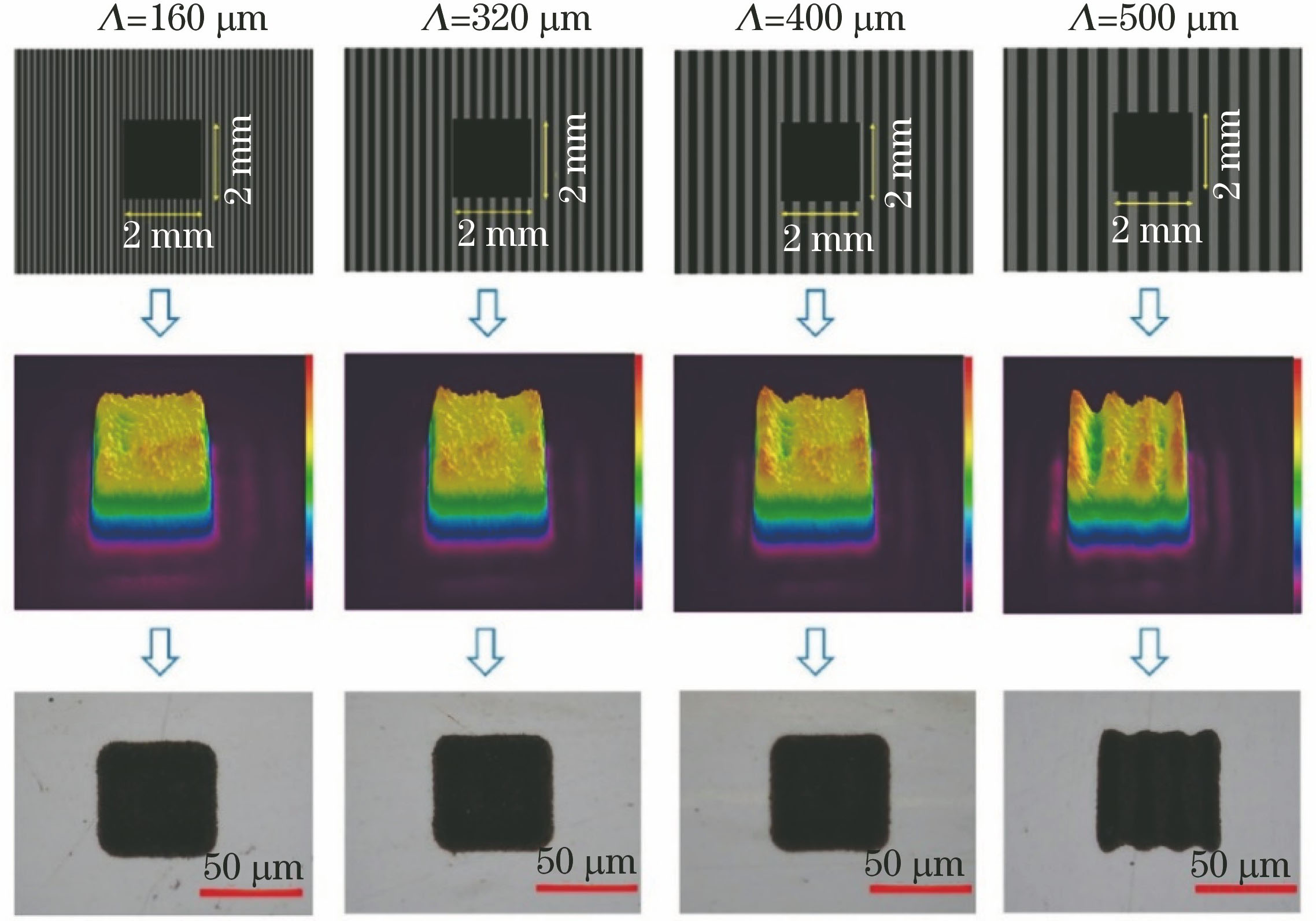
图 26. 实验结果。(a)(b)一张计算全息图在聚焦平面和离焦平面的光场仿真;(c) 20张计算全息图在离焦平面上的光场分布;(d)光场均匀性与全息图数(黑色方形)和离焦量(红色圆形)的关系[44]
Fig. 26. Experimental results. (a)(b)Optical intensity simulations of single-CGH at the focal plane and defocused plane; (c)optical intensity distribution at the defocused plane of 20 CGHs; (d)plot of optical uniformity as a function of number of CGHs (black square) and defocused position (red circle) [44]

表 1线偏振光、圆偏振光、径向偏振光和角向偏振光的产生方法[36]
Table1. Generation of linear, circular, radial, and angular polarized light[36]
|
孔德键, 孙小燕, 董卓林, 胡友旺, 段吉安. 飞秒激光空间光束整形加工技术研究进展[J]. 激光与光电子学进展, 2020, 57(11): 111416. Dejian Kong, Xiaoyan Sun, Zhuolin Dong, Youwang Hu, Ji'an Duan. Progress in Femtosecond Laser Processing Technology Based on Space Beam Shaping[J]. Laser & Optoelectronics Progress, 2020, 57(11): 111416.


 PDF全文
PDF全文

