1. INTRODUCTION
Microring resonators play a pivotal role in the success of silicon photonics; this is because silicon enables microring resonators of an unprecedented small size. To date, various silicon photonic devices, such as add–drop filters, tunable filters, electro-optic (E-O) modulators, optical delay lines, and biosensors, have been developed [1]. As active devices, silicon microring resonators have to rely on the relatively weak plasma dispersion effect to induce resonance wavelength tuning or E-O modulation, which are mostly achieved by using reversed PN junctions [2–9" target="_self" style="display: inline;">–9]. Such silicon photonic microring resonators usually possess E-O tuning efficiencies of 10–40 pm/V, which is suitable for high-speed E-O modulation. However, the resonance wavelength of a silicon microring is affected by process variations and temperature fluctuations, which cannot be sufficiently compensated for with the reversed PN junction structure, and require in-situ tuning and closed-loop compensations, which are usually achieved by free carrier injection using a PIN diode structure [10] or using thermal heaters [2,11,12]. Free carrier injection and thermal tuning can induce much larger resonance wavelength tuning, exceeding 100 pm/V or . Nevertheless, the high power dissipation at steady state limits their application especially for large-scale parallel optical links where hundreds and even thousands of microrings are needed.
In recent years, metal-oxide-semiconductor (MOS) microring resonator using hybrid III–V-on-Si has been reported [13]. It retains moderate E-O tuning efficiency (55 pm/V). Transparent conductive oxides (TCOs) such as indium-tin oxide (ITO) have attracted wide attention due to the dramatic tunability of their refractive indices owing to the strong plasma dispersion effect and large perturbation to the free carrier concentration [14]. A TCO material can even be tuned from being dielectric-like to metallic-like in the telecommunication wavelength range using a MOS capacitor structure. To date, several hybrid silicon–TCO photonic devices have been reported using straight waveguides [15], a Mach–Zehnder interferometer [16], and photonic crystal nanocavities [17]. However, TCO-gated silicon microring resonators have not been demonstrated. In this paper, we have designed and experimentally demonstrated a MOS-structured silicon microring filter with an ITO gate as the electric-tuning electrode. It achieved an ultralarge resonance wavelength tunability of 271 pm/V, which is obtained due to the reduced width (300 nm) of the ring waveguide and a 16-nm-thick high-dielectric-constant insulator. We demonstrated a broad resonance wavelength tuning range of over 2 nm with less than 12 ns of ultrafast response time and near-zero static power consumption, which can replace traditional thermal tuning for many on-chip optical interconnect applications.
2. DESIGN AND PRINCIPLE
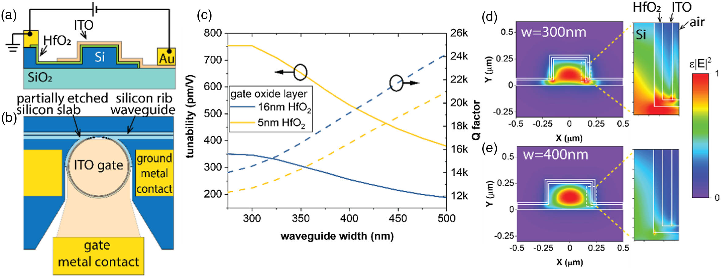
The tunable filter is driven by a hybrid TCO–silicon MOS capacitor operating in the carrier accumulation mode. As illustrated in Figs. 1(a) and 1(b), a 250-nm-thick p-type silicon rib waveguide serves as the bottom electrode of the MOS capacitor and a 50-nm-thick slab is used for electrical connections. The silicon microring is covered with as the gate oxide layer. On top of the gate oxide layer, a 20-nm-thick ITO layer acts as the top gate electrode. Because the entire microring is metal-free, we can build a high--factor microring resonator. Upon applying a negative bias on the ITO gate, electrons and holes accumulate at and interfaces, respectively. Plasma dispersion of the accumulated carriers in both ITO and silicon decreases the refractive indices, causing a blue shift of the resonance peaks. The plasma dispersion of a semiconductor follows the Drude model , where is the relative permittivity of the semiconductor, is the high-frequency permittivity, and is the collision frequency. The plasma frequency is related to the carrier density as , where is the vacuum permittivity, is the electron charge, and is the carrier effective mass. We can see that the change of permittivity is proportional to the change of carrier density . Next, the magnitude of resonance shift, , of the microring can be derived from the perturbation theory [18] as , where and are, respectively, the distribution of the initial and perturbed permittivities, and is the electric field distribution of the optical resonance mode. Then, the resonance shift is proportional to the total carriers accumulated per unit volume of the microring [19]. The two main factors that determine the tunability of a tunable microring filter are the capacitance density of the capacitor and the overlapping of the modulated carriers with the optical mode. First, electrically, the larger the capacitance density, the more the carrier density perturbation that can be induced with certain voltage, and, thus, the larger the tunability. A MOS capacitor offers additional freedom to control the capacitance density by controlling the thickness and dielectric constant of the gate oxide layer. Using thin high- material such as as the gate oxide layer, much larger capacitance density can be achieved compared with using a conventional reversed biased Si PN junction. Besides, unlike a carrier-injection-based PIN diode, in which a large carrier perturbation can also be achieved through heavy carrier injection, requiring large holding power consumption due to forward bias, the power consumption of a MOS capacitor is almost negligible. Second, optically, efficient tuning of the microring requires good overlapping of the accumulated carriers with the optical mode. For the hybrid TCO–silicon MOS capacitor configuration, carrier accumulation happens only at the ITO/oxide and silicon/oxide interfaces, which are away from the center of the optical mode. In order to improve the overlap, a narrower waveguide is preferred. We simulated the tunability of a microring with a radius of 12 μm as a function of waveguide width using the Lumerical MODE software, which is based on the finite-element method. The carrier density distribution in the accumulation layer was simulated by Silvaco and imported into Lumerical MODE. The result is plotted in Fig. 1(c). Tunability is calculated as , where is the effective index of the guided mode of the bent waveguide and is the resonance wavelength. Clearly, tunability increases as we decrease the waveguide width. Figures 1(d) and 1(e) show plots of simulated cross-sectional electrical energy distribution () of microrings with waveguide widths of 300 and 400 nm, respectively. Zoomed-in views of distributions in the interface region (white dashed box) are plotted on the right. We can see that for the narrower waveguide, the electrical energy at the interfaces is much larger. For the case of 16 nm of as the gate oxide layer, the tunability of the microring increases from 255 pm/V for the 400-nm-wide waveguide to 346 pm/V for the 300-nm-wide waveguide due to better overlapping. Moreover, tunability can be further improved by reducing the gate oxide thickness, which is inversely proportional to the capacitance density. For example, the tunability of the 300-nm-wide waveguide increases to 753 pm/V for layer thickness of 5 nm. Figure 1(c) also shows plots of the -factor of the simulated microring, which is calculated as [1]; here is the group index, is microring circumference, is the single-pass amplitude transmission, which can be calculated from waveguide loss (bending loss and free carrier dispersion loss), and is the self-coupling coefficient (assuming critical coupling condition ). For the 300-nm-wide waveguide with a 5 nm gate oxide layer, a high -factor of 12,000 is achievable. In simulation, the -factor of the microring is majorly limited by free carrier dispersion loss. The doping levels of p-Si and ITO used in the simulation are and , respectively.
Fig. 1. (a) Cross-sectional and (b) top view schematic of the hybrid TCO–silicon tunable microring filter. (c) Simulated tunability (solid lines) and -factor (dashed lines) of the tunable microring filters as functions of the waveguide width. Two different thicknesses of gate oxide layer are simulated (16 nm of and 5 nm of ). (d) and (e) Simulated cross-sectional electrical energy () distribution of the microring filter at different waveguide widths of 300 and 400 nm, respectively. Zoomed-in views of the distributions in the interface region (white dashed box) are plotted on the right.
下载图片 查看所有图片
3. FABRICATION AND CHARACTERIZATION
The device is fabricated on a 250-nm-thick silicon-on-insulator substrate with p-type background doping of . First, the waveguide, microring, and grating couplers are patterned by two steps of electron-beam lithography (EBL) and reactive-ion etching (RIE). The microrings have a radius of 12 μm each. Then, the contact region is highly doped by implantation with 5 keV of ions at a flux of , which corresponds to equivalent dopant concentrations of at the top 50-nm-thick silicon layer. After ion implantation, the dopant is activated by rapid thermal annealing at 1000°C for 10 s. Next, a 16-nm-thick layer is deposited by atomic layer deposition (ALD). After that, the ITO gate layer is patterned by EBL. A 20 nm layer of ITO is RF-sputtered under an mixed gas flow with 2% , followed by the liftoff process. Then, the gate oxide in the silicon contact region is removed with buffered hydrofluoric acid. After that, an Ni/Au electrode is evaporated and patterned by photolithography to form an ohmic contact with both p-type silicon and ITO. Finally, the sample is annealed at 275°C for 10 min. The fabricated device is shown in Fig. 2.
Fig. 2. (a) Optical image of a fabricated tunable microring filter with a radius of 12 μm. The ITO gate (highlighted by a red line) covers the majority of the microring except the coupling region. The ground electrodes are connected to the silicon ring through a partially etched silicon slab. (b) Scanning electron micrograph (SEM) of the fabricated silicon microring, showing side-wall roughness after the RIE process.
下载图片 查看所有图片
Light is coupled into and out of the silicon waveguide through the grating couplers from optical fibers. The fibers are mounted at a tilt angle of 10° each. A polarization controller is used at the input side to excite the TE mode. The output light is measured with an optical spectrum analyzer. A DC bias voltage is applied across the silicon waveguide and ITO gate. Figure 3(a) shows the transmission spectra of the 12 μm radius tunable microring filter with a 300 nm waveguide at different bias voltages. Resonance shift as a function of applied bias is shown in Fig. 3(b) (left axis). The microring filter exhibits almost linear resonance tuning for the applied negative bias, due to carrier accumulation. Under a positive bias, the tunability is smaller due to the depletion operation. Under a negative bias, average tuning efficiency of 216 pm/V is achieved. The largest tunability measured is from to , reaching 271.6 pm/V, which is the largest experimental tuning efficiency to the best of our knowledge. The value is less than the simulation results, which may be due to the deviation of the dielectric constant of the ALD layer from the ideal value used in the simulation. Under a large negative bias beyond , the tunability slightly decreases. We speculate that a large electrical field may force the accumulated electrons at the ITO interface into the layer, forming trapped charges, which effectively reduce the free carrier dispersion effect. However, the mechanism is still subject to further investigation. The tuning range of the tunable filter is determined by the dielectric strength of the gate oxide layer. In our testing, the 16-nm-thick layer breaks down slightly beyond a bias of (Fig. 4). This corresponds to a total resonance wavelength tuning range of more than 2 nm. The thermal-optical coefficient of silicon is around at 1.55 μm, which corresponds to a thermal tuning efficiency of . The tuning range of our microring filter can compensate for a thermally induced wavelength shift of around 20 K.
Fig. 3. (a) Measured transmission spectra of a tunable microring filter under different applied gate biases. The microring has a waveguide width of 300 nm and a gate oxide layer thickness of 16 nm. (b) Resonance shift (blue line, left axis) and -factor (red line, right axis) of the microring filter as functions of applied gate bias. (c) Simulated -factor of a microring with a waveguide width of 300 nm and 16 nm of gate oxide as a function of applied bias.
下载图片 查看所有图片
Fig. 4. Leakage current density of a testing MOS capacitor as a function of applied voltage with a 16-nm-thick gate oxide layer.
下载图片 查看所有图片
Figure 3(b) also shows plots of the -factor of the microring as a function of applied bias. A relatively low -factor of is measured at 0 V bias, due to optical scattering loss induced by the rough side wall as shown in Fig. 2(b), which is limited by our EBL and dry etching processes. The narrower waveguide design also makes our microring resonator more vulnerable to surface roughness. This issue can be solved in the future by using commercial silicon photonics foundry to obtain high quality, low-loss passive optical devices. We also observed that with increase in the negative bias, the -factor gradually decreases, since refractive modulation by the plasma dispersion effect is always accompanied by free carrier absorption. To evaluate how free carrier absorption will affect the -factor in the biased condition, we simulated the -factor of a microring with a waveguide width of 300 nm and 16 nm of gate oxide as a function of applied bias in Fig. 3(c). It shows that the -factor decreases significantly. However, it is still possible to maintain a reasonable -factor of above 5000 for at least a wavelength tuning range of 1 nm. To further increase the wavelength tuning range, high-mobility TCO materials such as CdO with smaller free carrier loss, as suggested in Ref. [20], have to be used to replace ITO as the gate layer for the MOS structure.
The static power consumption of the TCO–silicon tunable microring filter is only determined by the leakage current, which is below the noise level of our measurement tool (). Figure 4 shows leakage current density as a function of gate voltage for a testing MOS capacitor with a large area and the same 16-nm-thick gate oxide layer. The capacitor exhibits a leakage current density of at bias. Then, we can calculate the leakage current of the tunable microring filter to be at bias, which indicates near-zero (0.16 pW) static power consumption. Additionally, carrier accumulation is a fast process. The speed of the microring is only limited by the resistance–capacitance delay. Figures 5(a) and 5(b) show the AC response of our tunable filter at 20 kHz. Over 20 dB of modulation depth is measured. Figures 5(c) and 5(d) show plots of the rising and falling edges of Fig. 5(b), respectively. The rising and falling time is , which is much faster than those in traditional thermal tuning.
Fig. 5. (a) Voltage swing of 0 to applied on the tunable microring filter. (b) Output response of the microring filter. (c) and (d) Rising and falling edge of the output in (b), respectively.
下载图片 查看所有图片
4. CONCLUSION
In conclusion, we designed and fabricated a silicon microring resonator gated by an ITO electrode. Benefitting from a high capacitance density and a narrow microring waveguide, it achieved an ultralarge resonance wavelength tunability of 216–271 pm/V. We demonstrated a broad resonance wavelength tuning range of over 2 nm with less than 12 ns of ultrafast response time and near-zero static power consumption. These TCO-gated tunable microring filters can replace traditional thermal tuning for on-chip wavelength-division multiplexing optical interconnects.
5 Acknowledgment
Acknowledgment. The authors would like to acknowledge the support of the EM Facility and MaSC center at Oregon State University for device fabrication. We also thank Dr. Zhihong Huang and Dr. Di Liang at Hewlett Packard Labs for helpful discussion.
Erwen Li, Behzad Ashrafi Nia, Bokun Zhou, Alan X. Wang. Transparent conductive oxide-gated silicon microring with extreme resonance wavelength tunability[J]. Photonics Research, 2019, 7(4): 04000473.


