1. INTRODUCTION
Radio frequency (RF) switches are essential for implementing routing of RF signals and are widely applied in modern communication and radar systems [13" target="_self" style="display: inline;">–3]. The conventional solutions with practical compact forms are generally based on micro-electromechanics or employing solid-state PIN-diode or active-device switches [46" target="_self" style="display: inline;">–6]. Although allowing for various designs, these solutions are faced with an important challenge raised by the ever-increasing demand for RF signal frequency and bandwidth, i.e., sub-nanosecond or faster switching speeds. The difficulty of implementation stems from the limitations of material properties or the lack of tunability of the electrical circuits [6]. Alternatively, microwave photonics provides a promising path to overcome the bottleneck, where the inherent advantages of photonics such as wide bandwidth, easy tuning mechanism, a diversity of light wave interaction properties for signal carrying and processing, and low electromagnetic interference can be utilized for RF engineering to enable new breakthroughs in performance and features [7–10" target="_self" style="display: inline;">–10]. Regarding photonic implementations of RF switches, several previous proposals using discrete components have demonstrated the functions of amplitude and frequency switching at speeds down to tens of picoseconds [11,12]. In general, these methods use electro-optical phase modulators incorporated in an optical fiber-based interferometer, which features flexible system composition and allows for the use of various tuning mechanisms, e.g., in the frequency domain or polarization domain. These works manifest the value and potential of microwave photonics. From a practical point of view, commercial adoption of photonic RF solutions also requires the motivations of easy implementation, high robustness, low power consumption, as well as fabrication cost. In addition, functional reconfigurability is also a desirable feature to facilitate new innovations of flexible systems. In this context, silicon photonics is a promising technology platform. The recent development has demonstrated remarkable capabilities such as compact passive devices with bend radii in the order of a few micrometers (μm) [13–16" target="_self" style="display: inline;">–16], high-efficiency modulators and photodiodes with bandwidth of tens of gigahertz (GHz) [17,18], and potential for hybrid electronics-photonics integration [19,20].
Here we propose and verify a photonic implementation of an RF switch. It is not only able to perform switching at a sub-nanosecond speed but can also provide options of frequency doubling of the input RF signals, allowing for very flexible output waveforms. The core device is a traveling-wave silicon modulator (TW-Si-mod) with a size of and a modulation bandwidth of 10 GHz. Our implementation also features low complexity, high stability, easy control, and potential for full integration. Using two microwave frequencies, i.e., 15 GHz and 20 GHz, as two simultaneous RF input signals, we experimentally demonstrate their amplitude and frequency switching as well as that of the doubled frequencies, i.e., 30 GHz and 40 GHz, with a switching frequency of5 GHz.
2. DEVICE PRINCIPLE
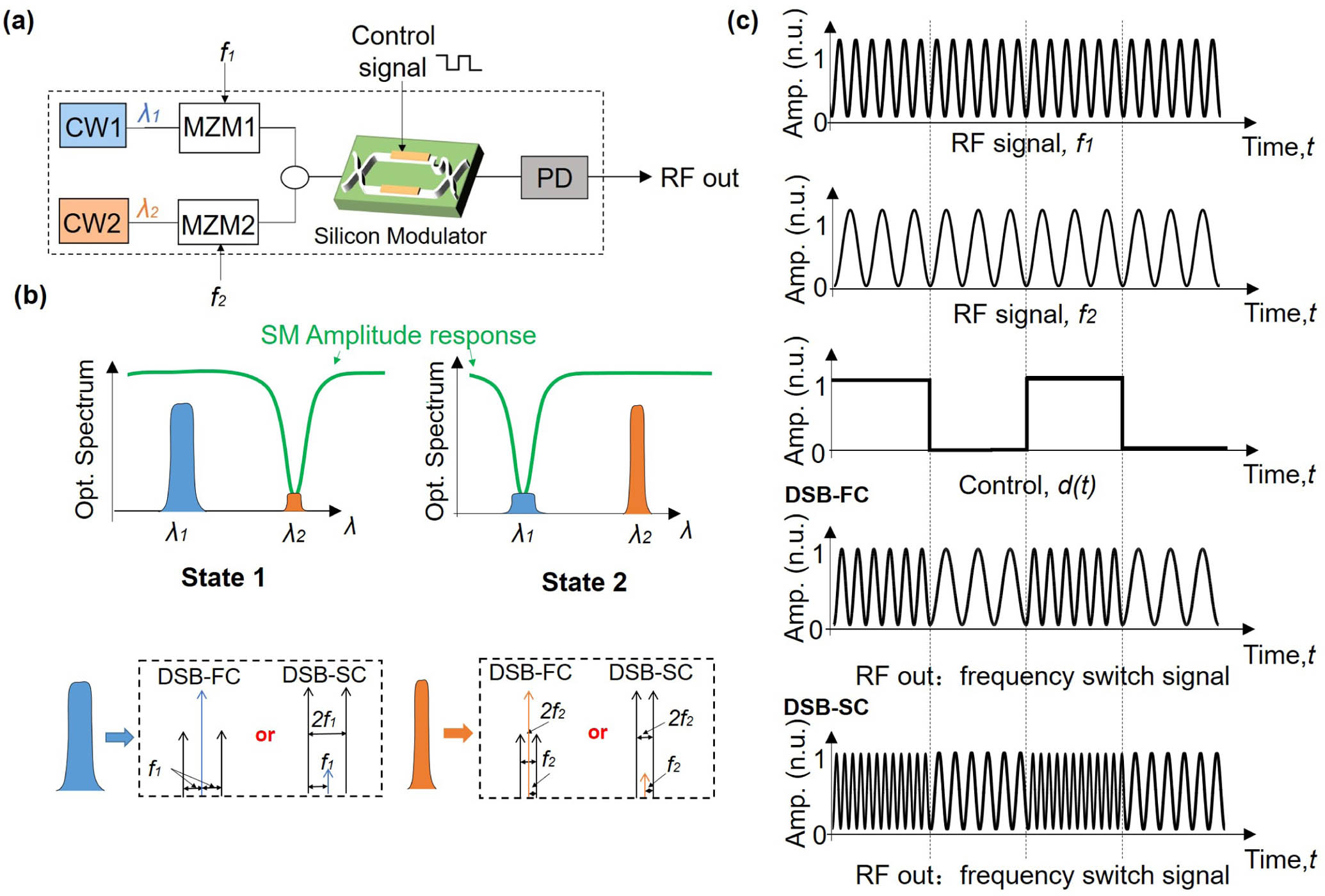
Figure 1 shows the system’s working principle. As shown in Fig. 1(a), the system comprises two CW lasers with wavelengths and , two Mach–Zehnder modulators (MZMs) for upconverting the input RF signals, i.e., and , to the optical domain, a particular TW-Si-mod as the core-switching mechanism, and a photodiode for downconverting the modulated and processed optical signals to the RF domain and delivering the switching RF signal to the system output. Figures 1(b) and 1(c) illustrate the signal processing steps in the frequency and time domain, respectively. For the upconversion of the input RF signals, two different kinds of modulation spectra can be used in our system, i.e., the double-sideband full-carrier (DSB-FC) spectrum and double-sideband suppressed-carrier (DSB-SC) spectrum [21], the implementation of which is conducted by means of properly configuring the bias of the MZM. Next, the two modulated wavelengths are multiplexed into one signal, which is then sent to the TW-Si-mod. The TW-Si-mod is a notch filter with its central frequency governed by the voltage of an electrical control signal (modulator driving signal). When and are frequency aligned with the filter notch as shown in Fig. 1(b), the modulator allows the switching of these two wavelengths, namely, passing one and suppressing the other at a time. Then, by means of a photodiode, the switching of the optical signals is transferred to the switching of RF signals. In particular, the choice of DSB-FC or DSB-SC modulation leads to the frequency reconfigurability between the original RF frequencies (i.e., and ) or doubled frequencies (i.e., and ) at the output.
Fig. 1. (a) Schematic of the frequency-switch generation system using the proposed photonic method. (b) A frequency-domain illustration of the system working principle. (c) A time-domain illustration of the signal waveforms.
下载图片 查看所有图片
The corresponding mathematical expressions of the system are given in the following. The modulated optical signals at the outputs of the MZMs, , can be described as where is the amplitude coefficient determined by the input optical power and modulator insertion loss, and are the corresponding frequencies of and , and is the input frequency. is the th-order Bessel function of the first kind, and is the modulation index determined by the ratio between the amplitude of the input RF signal and the half-wave voltage of the MZM [22]. Here we assume a small-signal scenario where , and thereby only and that describe the carrier and first-order sidebands are significant frequency components within consideration. For the case of DSB-SC, is suppressed to a negligible value compared with , and thereby Eq. (1) reduces to The TW-Si-mod is composed of a delay line filter with an electro-optical phase modulator in one of its arms as shown in Fig. 2(a). It breaks down to three constituent subsections, namely, two 3 dB directional couplers and a delay section between them. The transfer function of the modulator can be given as [23] where denotes the amplitude coefficient, is the delay difference between the two arms that determines the filter free spectral range (FSR) by , and is a phase shift determined by a modulating signal in volts and modulator half-wave voltage [16]. We assume that is a binary digital signal, and its on-off status results in two frequencies of the filter notch as illustrated in the green lines in Fig. 1(b). Here we use port X1 as the input and port Y1 as the output. Then, after detection in the photodiode, the output RF signal in terms of photocurrent can be expressed by where where is the amplitude coefficients and is the responsivity of the PD. When shifts from “1” to “0,” optical frequency shifts from to .
Fig. 2. (a) The schematic and (b) photomicrograph of the silicon modulator. (S, signal; G, ground.)
下载图片 查看所有图片
In practice, the filter notch should have a strong suppression over the entire modulated spectrum of each wavelength in order to perform a clean “switch-off.” Besides, the FSR of the filter should be such that it introduces negligible suppression to the “switch-on” wavelength to maximize the signal-to-noise ratio.
3. CHIP DESIGN AND CHARACTERIZATION
Figure 2(a) shows the schematic of TW-Si-mod. It consists of four subsections, namely, two directional couplers and a phase-shifting subsection in between with two arms of delay difference subsection. Figure 2(b) shows a photomicrograph of the TW-Si-mod. The device is fabricated on a silicon-on-insulator (SOI) wafer with 200 nm top silicon and 2 μm buried oxide [24], using a multi-project wafer (MPW) foundry fabrication service run under the ePIXfab ISIPP25G silicon technology platform (MZMCTE_TWLAB_450_1500). The device has dimensions of and an inter-arm length difference of 0.04 mm, corresponding to an FSR of about 1.75 THz (14 nm). The phase shifter is 1.5 mm. From the datasheet, the theoretical S21 3 dB electro-optic (EO) bandwidth is 11.3 GHz at , and Vπ is 8.5 V at bias of −2 V. The phase shifter propagation loss is about 12 dB/cm. The total insertion loss of the device is about 7 dB including on-chip loss of 2 dB, and couple-in and couple-out loss is about 5 dB. The chip sits on a thermal island with vias to the base layer, underneath which is a Peltier element to control the chip’s temperature. For the implementation of the phase modulator, the symmetric lateral PN diodes are embedded along the arms, operating with high-speed, free-carrier depletion mode under reverse bias conditions. These enable modulation of the refractive index and thus modify the modulator spectral shape, i.e., shifting its frequency of the notch. One side of the RF signal connectors is connected with 50 Ω resistors to enable the traveling-wave modulation. Here a tunable 50 Ω resistor is externally connected to the end of the TW-Si-MOD so that the modulation efficiency can be optimized. Figure 3(a) shows the electrical -parameter measurement of the modulator by means of a vector network analyzer (ANRITSU 37247D). The result shows a transmission () 3 dB bandwidth of 10 GHz. The reflection () is less than up to 20 GHz. As a verification of the transmission bandwidth, the inset in Fig. 3(a) shows an eye diagram measurement, which presents an open eye opening at 10 Gb/s. The spectral shapes of the TW-Si-mod for different bias voltages are shown in Fig. 3(b), and they were measured using a LUNA two-port optical analyzer (VOA5000 with a resolution of 160 MHz). The present switch operates with the carrier-injection mode. The 30 dB bandwidth of the notch is about 50 GHz (0.4 nm). In practice, the notch bandwidth can be reduced by employing a ring modulator with different orders and configurations. By tuning the bias voltage from 0 to 2 V, the notch shifts by 1.12 THz (9 nm). The applied voltage causes carrier concentration to vary, leading to the increase of the loss of the phase shifter. As a result, the extinction ratio (ER) of the TW-Si-mod decreases when the losses of the two arms are not balanced [25]. Nevertheless, during the entire shifting process, the notch depth remains larger than 30 dB, which is enough for signal suppression.
Fig. 3. (a) Electro-optical bandwidth measurements of the TW-Si-mod (with a bias of 0 V). (b) Measured power transmissions of the TW-Si-mod for different bias voltages.
下载图片 查看所有图片
4. EXPERIMENTAL RESULTS
Figure 4 illustrates the experiment setup for the proposed RF switch function. Two CW lasers with wavelengths of 1556.5 nm and 1564.5 nm are used as the light sources, each feeding an MZM (Thorlabs LN05S-FC). The wavelengths of the two lasers are chosen to achieve the best ER performance of the TW-Si-mod. The laser frequency shift is only several megahertz (MHz), which is far smaller than the frequency separation of two RF signals. Two laser frequencies are aligned with the peak and notch of the spectrum in the TW-Si-mod to pass the useful signal and stop the unneeded signal. Two RF frequencies, i.e., and (each generated using a Rohde & Schwarz SMF 100A RF synthesizer), are used as the two inputs to drive the two MZMs. The measured optical spectra after wavelength multiplexing are shown in Fig. 5. For the DSB-FC case, the MZM is working at the 3 dB transmission point and using , which is around 1.75 V [26]. For the DSB-SC case, the MZM is working at the minimum transmission point and using , which is around 3.5 V [26]. Figures 5(a)–5(c) are the DSB-FC modulated optical spectra at the input of the TW-Si-mod and at the output with one of the two wavelengths suppressed by the notch. Likewise, Figs. 5(d)–5(f) are with DSB-SC modulation, with a carrier suppression ratio about . The TW-Si-mod uses grating couplers optimized for TE polarization and was given an optical input power of 10 dBm delivered through a combination of an erbium-doped fiber amplifier (EDFA) and a polarization controller. For the switching, the binary control signal to the TW-Si-mod is such that the low-voltage (level “0”) status aligns the notch to suppress signal with wavelength 1564.5 nm and the high-voltage (level “1”) status suppressing signal with wavelength 1556.5 nm. The measured wavelength suppression ratio in this work is about , which effectively overcomes the switch crosstalk.
Fig. 4. Experimental setup of the proposed millimeter (mm)-wave frequency-switch system. (ECL, external cavity laser; PC, polarization controller; PPG, pulse pattern generator; EDFA, erbium-doped fiber amplifier; WSS, waveshaper; PD, photodiode.)
下载图片 查看所有图片
Fig. 5. Power transmissions before TW-Si-mod, after TW-Si-mod with control signal on and off, (a)–(c) when both external MZMs are biased at quadrature transmission point, (d)–(f) when both external MZMs are biased at minimum transmission point. (RF seed frequencies are 20 GHz and 15 GHz.)
下载图片 查看所有图片
Figure 6 shows the RF output waveforms according to different system settings. These are measured using a real-time 50 GHz oscilloscope (Agilent DSO-X-95004Q). Figures 6(a) and 6(b) are the waveforms routing out of the PD without the chip with DSB-FC and DSB-SC modulation, respectively, for input frequencies and . The doubled frequencies, 40 GHz and 30 GHz, are shown in Figs. 6(c) and 6(d). Figure 6 shows the frequency-switching performance of the proposed microwave photonic (MWP) RF switch, measured by a 50 GHz oscilloscope. A binary control signal at 5 Gb/s with a pattern of “010101” sequence and a peak-peak voltage of 1.8 V was applied to drive the TW-Si-mod as a control signal, and the waveforms of the control signal are shown in the upper figures in Figs. 7(a) and 7(b).
Fig. 6. Waveform measurements of generated RF signals without chip: (a) and (b) with DSB-FC modulation; (c) and (d) with DSB-SC modulation. (RF seed frequencies are 20 GHz and 15 GHz.)
下载图片 查看所有图片
Fig. 7. Waveform measurements of generated RF signals modulated by a square wave signal: (a)–(c) with DSB-FC modulation; (d)–(f) with DSB-SC modulation. (RF seed frequencies are 20 GHz and 15 GHz.)
下载图片 查看所有图片
In Fig. 7(a), the two modulators are working at DSB-FC modulation. The MWP notch filter is first aligned at when no control signal is applied, i.e., the sinusoidal signal is blocked by the notch filter, while passes through the RF switch. The peak voltage of the control signal is set to 2 V such that the filter notch is tuned away from and aligned at during the high-voltage period of the square wave, allowing the input RF signal to completely pass through the RF switch while blocking the RF signal. The powers of the two lasers are tuned to compensate for the extinction ratio and bias-induced loss difference between the two stages of the TW-Si-mod. As a result of applying a 5 Gb/s square control signal to the RF switch, the two input 15 GHz and 20 GHz RF signals are switched periodically with an ON-state and OFF-state duration of 200 ps as shown in Fig. 7(a). Similarly, Fig. 7(b) shows the RF signals that are switching between the two RF signals (40 GHz and 30 GHz) when two MZMs are working in DSB-SC modulation. Figures 7(b), 7(c) and 7(e), 7(f) show the input laser is switched ON and OFF periodically for DSB-FC and DSB-SC modulation, respectively. The output signal is a linear superposition of two RF signals carried on the two CW wavelengths. The two wavelengths do not need to be phase locked, as their frequency spacing is far beyond the bandwidth of the PD. As shown in Fig. 7, the switch has an ON-OFF transition time of 50 ps in agreement with that of the control signal. A faster TW-Si-mod could be used to perform instant switching in accordance with the binary control signal. Besides, amplitude fluctuation is seen in the output signal. This is because the random phase may occur due to the independence of the two input RF signals; the dynamics of the TW-Si-mod when switching between two steady resonance states also contributes to the amplitude variation of the generated RF signal, and the notch of the TW-Si-mod provides slightly different power suppressions for the two RF signals during the shifting between two states. This can be improved by using additional amplitude control of the input RF signals or designing a TW-Si-mod with a larger bandwidth.
5. CONCLUSION
We have experimentally demonstrated a photonic implementation of a high-speed RF switch. The switching mechanism uses a TW-Si-mod featuring high device compactness and power efficiency. Our solution provides not only RF-switching function at a sub-nanosecond speed but also provides the option of frequency doubling. While our experiment shows an RF output frequency up to 40 GHz, the TW-Si-mod can be designed with a spectral shape featuring a larger FSR and thereby allows for RF frequencies only limited by the bandwidths of MZMs, PDs, and other electrical devices used in the system, implying a possible frequency extension to the X band (). At this stage, we only integrated the key components of the RF switch on the chip for proof of concept; the main challenge to implement a fully integrated RF signal generator is to find the proper single or hybrid material to support both passive and active components and ensure the good quality of each component. Recent development of silicon technology has demonstrated modulators with higher bandwidths and a range of functions that cover all the constituent components of our system [27]. In addition, a ring resonator can work as a notch filter and offer ultra-compactness. In future studies, we will also look into designing ring modulators of different orders and configurations with high ER to optimize the RF switch’s performance and size. Therefore, further development may consider implementations of faster switching capabilities using a fully compact integrated device, which points to a promising solution for a high-speed, reconfigurable RF switch on a chip scale.
6 Acknowledgment
Acknowledgment. The design of the chip and experimental work was performed at Monash University, Australia. We thank Prof. Arthur Lowery from Monash University for the assistance in the experiments. P.J. acknowledges the Startup Fund of the Hundred Talent Program at the Zhejiang University, China.
Yiwei Xie, Leimeng Zhuang, Pengcheng Jiao, Daoxin Dai. Sub-nanosecond-speed frequency-reconfigurable photonic radio frequency switch using a silicon modulator[J]. Photonics Research, 2020, 8(6): 06000852.
 Download: 799次


