Photonics Research, 2020, 8 (6): 06000768, Published Online: Apr. 29, 2020
Highly luminescent and stable lead-free cesium copper halide perovskite powders for UV-pumped phosphor-converted light-emitting diodes Download: 989次
Figures & Tables
Fig. 1. (a) Schematic illustration of synthetic process of Cs 3 Cu 2 I 5 perovskite powder by using a planetary ball mill. (b) SEM image of Cs 3 Cu 2 I 5 perovskite powder with inset showing size distribution. (c) TEM image of Cs 3 Cu 2 I 5 perovskite. (d) HRTEM image of Cs 3 Cu 2 I 5 perovskite along with an inset of SAED pattern of Cs 3 Cu 2 I 5 perovskite crystal. (e) EDX spectrum and elemental content analysis of obtained Cs 3 Cu 2 I 5 perovskite. (f) SEM image and EDX elemental mapping (g) Cs, (h) Cu, and (i) I of the selected Cs 3 Cu 2 I 5 perovskite powder.
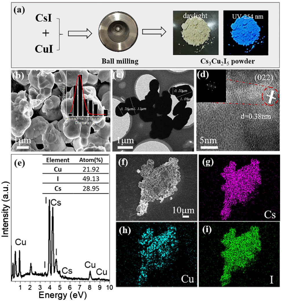
Fig. 2. (a) XRD pattern of obtained Cs 3 Cu 2 I 5 powder, compared with the orthorhombic bulk Cs 3 Cu 2 I 5 at the bottom (JCPDS No. 45-0077). (b) TGA curve of Cs 3 Cu 2 I 5 powder. (c) XPS survey spectrum and HRXPS spectra of (d) Cs 3d, (e) Cu 2p, and (f) I 3d in Cs 3 Cu 2 I 5 powder.
Fig. 3. (a) PL spectra of Cs 3 Cu 2 I 5 powder under different excitation wavelengths from 260 to 340 nm. (b) PLE spectra measured at different PL peaks ranging from 400 to 480 nm. (c) UV-Vis diffuse reflectance spectrum of the Cs 3 Cu 2 I 5 powder; the inset shows the Tauc plot used for the bandgap estimation. (d) Time-resolved PL decay curve of Cs 3 Cu 2 I 5 powder excited by the laser of 300 nm. (e) Crystal structure of Cs 3 Cu 2 I 5 , as viewed down the a axis (green, purple, and blue balls indicate Cs, I, and Cu atoms, respectively). (f) DOS plots of the Cs 3 Cu 2 I 5 powder. (g) Calculated electronic band structure of Cs 3 Cu 2 I 5 ; the Fermi energy is set to E = 0 and denoted with an orange dash line. (h) Configuration coordinate diagram for the excited-state reorganization; the violet and blue arrows represent transition and radiation processes, respectively, and the black arrow represents intersystem crossing.
Fig. 4. (a) Integrated PL intensity as a function of temperatures from 25°C to 300°C. Variation of PL intensity of Cs 3 Cu 2 I 5 (b) at 100°C and (c) under a xenon lamp irradiation over time. (d) XRD patterns of Cs 3 Cu 2 I 5 exposed to air for three months. (e) PL intensity of Cs 3 Cu 2 I 5 exposed to air for three months.
Fig. 5. (a) SEM image of Cs 3 Cu 2 Cl 5 perovskite powder. (b) HRTEM image of Cs 3 Cu 2 Cl 5 perovskite along with an inset of SAED pattern of Cs 3 Cu 2 Cl 5 perovskite crystal. (c) EDX elemental mappings of Cs 3 Cu 2 Cl 5 powder; the scale bar is 10 μm. (d) XRD pattern of Cs 3 Cu 2 Cl 5 powder with standard JCPDS cards (Cs 3 Cu 2 Cl 5 , 24-0247 and CsCl, 05-0607). (e) XPS survey spectrum of Cs 3 Cu 2 Cl 5 powder. HRXPS analysis of Cs 3 Cu 2 Cl 5 powder: (f) Cs 3d spectrum, (g) Cl 2p spectrum, and (h) Cu 2p spectrum. (i) TGA curve of Cs 3 Cu 2 Cl 5 powder.
Fig. 6. (a) Normalized UV-Vis absorption (purple dash line) and PL (green solid line) spectra of the as-obtained Cs 3 Cu 2 Cl 5 powder; inset: green emission image under UV-254 nm lamp. (b) Normalized PLE spectra measured over different PL peaks ranging from 470 to 550 nm. (c) Time-resolved PL decay curve of the Cs 3 Cu 2 Cl 5 powder detected at 510 nm with excitation of 300 nm. (d) Crystal structure of Cs 3 Cu 2 Cl 5 , as viewed down the a axis (green, brown, and blue balls indicate Cs, Cl, and Cu atoms, respectively). (e) DFT electronic band structure of Cs 3 Cu 2 Cl 5 with a direct bandgap (2.45 eV). (f) XRD patterns of Cs 3 Cu 2 Cl 5 exposed to air for two months.
Lingling Xie, Bingkun Chen, Fa Zhang, Ziheng Zhao, Xinxin Wang, Lijie Shi, Yue Liu, Lingling Huang, Ruibin Liu, Bingsuo Zou, Yongtian Wang. Highly luminescent and stable lead-free cesium copper halide perovskite powders for UV-pumped phosphor-converted light-emitting diodes[J]. Photonics Research, 2020, 8(6): 06000768.