二维光子晶体全光逻辑门的设计与仿真  下载: 1272次
Design and Simulation of Two-Dimensional Photonic Crystal All-Optical Logic Gates
1 兰州交通大学电子与信息工程学院, 甘肃 兰州 730070
2 兰州交通大学光电技术与智能控制教育部重点实验室, 甘肃 兰州 730070
图 & 表
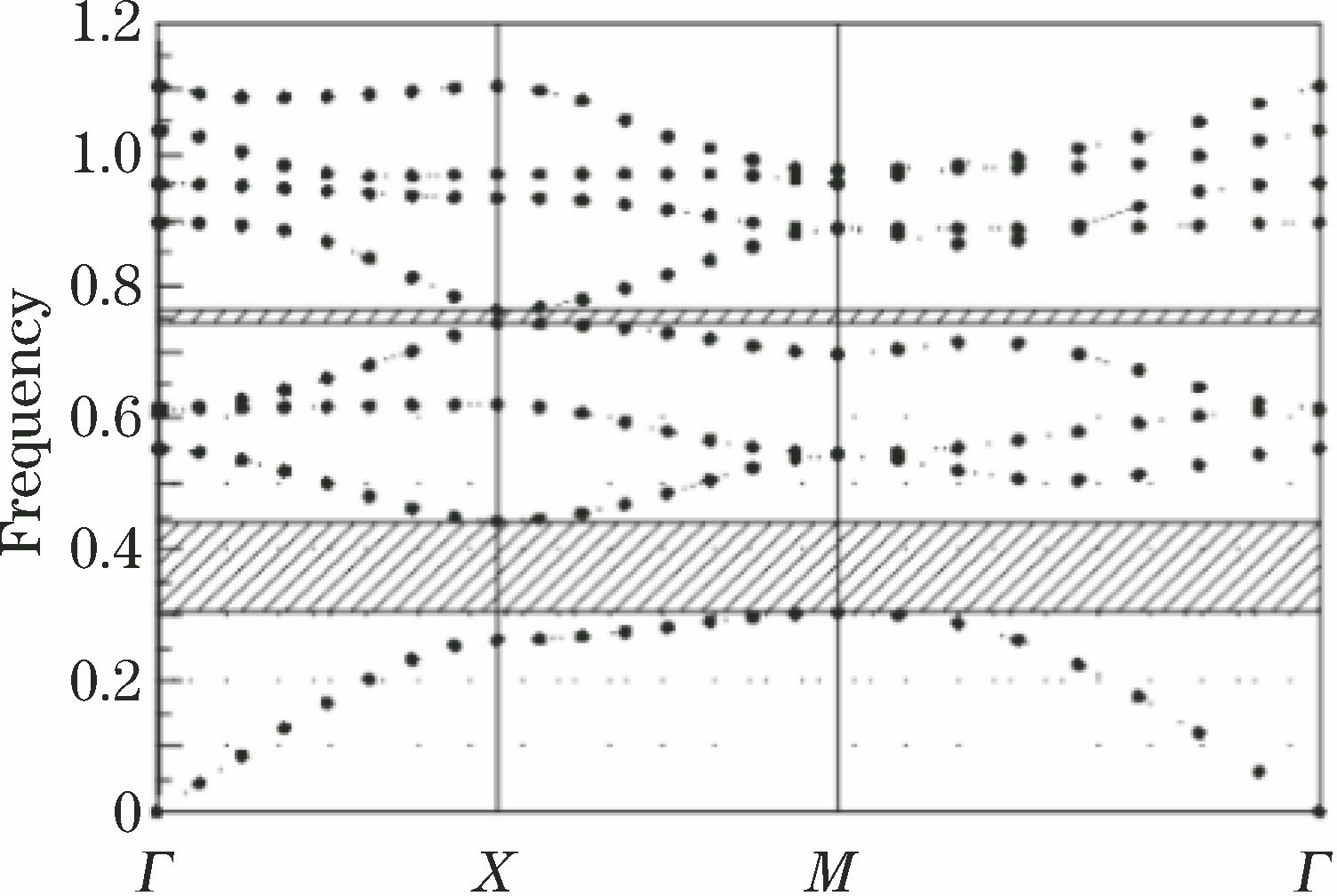
图 1. 完整光子晶体能带图
Fig. 1. Energy band structure of complete photonic crystal
下载图片 查看原文
图 2. 光子晶体或门结构
Fig. 2. Structure of OR gate of photonic crystal
下载图片 查看原文
图 3. 或门的模拟场分布图。(a) IA=0,IB=1;(b) IA=1,IB=0;(c) IA=1,IB=1
Fig. 3. Simulated field distributions of OR gate. (a) IA=0, IB=1; (b) IA=1, IB=0; (c) IA=1, IB=1
下载图片 查看原文
图 4. 或门的性能变化图。(a)输出端透射率分布;(b)时间响应曲线
Fig. 4. Performance variations of OR gate. (a) Transmittance of out port; (b) curve of time response
下载图片 查看原文
图 5. 光子晶体与门结构
Fig. 5. Structure of AND gate of photonic crystal
下载图片 查看原文
图 6. 与门的模拟场分布图。(a) IA=0,IB=1;(b) IA=1,IB=0;(c) IA=1,IB=1
Fig. 6. Simulated field distributions for AND gate. (a) IA=0, IB=1; (b) IA=1, IB=0; (c) IA=1, IB=1
下载图片 查看原文
图 7. 与门的性能变化图。(a)输出端透射率分布;(b)时间响应曲线
Fig. 7. Performance variations of AND gate. (a) Transmittance of out port; (b) curve of time response
下载图片 查看原文
图 8. 光子晶体异或门结构
Fig. 8. Structure of XOR gate of photonic crystal
下载图片 查看原文
图 9. 异或门的模拟场分布图。(a) IA=0,IB=1;(b) IA=1,IB=0;(c) IA=1,IB=1
Fig. 9. Simulated field distributions of XOR gate. (a) IA=0, IB=1; (b) IA=1, IB=0; (c) IA=1, IB=1
下载图片 查看原文
图 10. 异或门的性能变化图。(a)输出端透射率分布;(b)时间响应曲线
Fig. 10. Performance variations of XOR gate. (a) Transmittance of out port; (b) curve of time response
下载图片 查看原文
图 11. 光子晶体或非门结构
Fig. 11. Structure of NOR gate of photonic crystal
下载图片 查看原文
图 12. 或非门的模拟场分布图。(a) IA=0,IB=0;(b) IA=0,IB=1;(c) IA=1,IB=0;(d) IA=1,IB=1
Fig. 12. Simulated field distributions of NOR gate. (a) IA=0, IB=0; (b) IA=0, IB=1; (c) IA=1, IB=0; (d) IA=1, IB=1
下载图片 查看原文
图 13. 或非门的性能变化图。(a)输出端透射率分布;(b)时间响应曲线
Fig. 13. Performance variations of NOR gate. (a) Transmittance of out port; (b) curve of time response
下载图片 查看原文
图 14. 光子晶体与非门结构
Fig. 14. Structure of NAND gate of photonic crystal
下载图片 查看原文
图 15. 与非门的模拟场分布图。(a) IA=0,IB=0;(b) IA=0,IB=1;(c) IA=1,IB=0;(d) IA=1,IB=1
Fig. 15. Simulated field distributions of NAND gate. (a) IA=0, IB=0; (b) IA=0, IB=1; (c)IA=1, IB=0; (d)IA=1, IB=1
下载图片 查看原文
图 16. 与非门的性能变化图。(a)输出端透射率分布;(b)时间响应曲线
Fig. 16. Performance variations of NAND gate. (a) Transmittance of out port; (b) curve of time response
下载图片 查看原文
表 1或门真值表
Table1. Truth table of OR gate
| IA | IB | Output logic | Transmittance |
|---|
| 0 | 0 | 0 | 0 | | 0 | 1 | 1 | 0.7714 | | 1 | 0 | 1 | 0.6976 | | 1 | 1 | 1 | 0.9969 |
|
查看原文
表 2与门真值表
Table2. Truth table of AND gate
| IA | IB | Output logic | Transmittance |
|---|
| 0 | 0 | 0 | 0 | | 0 | 1 | 0 | 0.1330 | | 1 | 0 | 0 | 0.1621 | | 1 | 1 | 1 | 0.9895 |
|
查看原文
表 3异或门真值表
Table3. Truth table of XOR gate
| IA | IB | Output logic | Transmittance |
|---|
| 0 | 0 | 0 | 0 | | 0 | 1 | 1 | 0.5571 | | 1 | 0 | 1 | 0.7349 | | 1 | 1 | 0 | 0.0895 |
|
查看原文
表 4或非门真值表
Table4. Truth table of NOR gate
| IA | IB | Output logic | Transmittance |
|---|
| 0 | 0 | 1 | 0.6897 | | 0 | 1 | 0 | 0.2420 | | 1 | 0 | 0 | 0.1969 | | 1 | 1 | 0 | 0.1284 |
|
查看原文
表 5与非门真值表
Table5. Truth table of NAND gate
| IA | IB | Output logic | Transmittance |
|---|
| 0 | 0 | 1 | 0.5989 | | 0 | 1 | 1 | 0.6488 | | 1 | 0 | 1 | 0.7349 | | 1 | 1 | 0 | 0.0950 |
|
查看原文
刘振, 吴蓉, 严清博, 吴小所. 二维光子晶体全光逻辑门的设计与仿真[J]. 激光与光电子学进展, 2019, 56(18): 182301. Zhen Liu, Rong Wu, Qingbo Yan, Xiaosuo Wu. Design and Simulation of Two-Dimensional Photonic Crystal All-Optical Logic Gates[J]. Laser & Optoelectronics Progress, 2019, 56(18): 182301.


 PDF全文
PDF全文

