Chinese Optics Letters, 2019, 17 (12): 122401, Published Online: Nov. 26, 2019   

Broadband mid-IR antireflective Reuleaux-triangle-shaped hole array on germanium Download: 989次

Author Affiliations
1 Beijing Key Laboratory of Nanophotonics and Ultrafine Optoelectronic Systems, Key Laboratory of Photoelectronic Imaging Technology and System, Ministry of Education, School of Optics and Photonics, Beijing Institute of Technology, Beijing 100081, China
2 Yunnan KIRO - CH Photonics Co., Ltd., Kunming 650223, China
3 School of Materials Science & Engineering, Beijing Institute of Technology, Beijing 100081, China
Abstract
A gradient-index Reuleaux-triangle-shaped hole array was fabricated on germanium (Ge) by nanoimprint lithography and inductively coupled plasma processing as a broadband mid-infrared (IR) antireflective surface. The interaction between the {111} planes of cubic crystalline Ge and a circular mold successfully produced an orderly and periodically distributed Reuleaux-triangle-shaped hole array. As a result, the average transmittance increased 15.67% over the waveband at 3–12 μm and remained stable at the incidence angle of up to 60°. The vertices of the Reuleaux triangle showed local enhancement of the electric field intensities due to interference of the incident and reflected radiation fields. It was also found that nonuniform hole depths acted to modulate the transmittance over the 3–12 μm waveband.

Monocrystalline germanium (Ge) is a preferred lens and window material for high-performance infrared (IR) imaging systems because of its high refractive index and broadband transparency (1.8–25 μm) in the IR region. Broadband antireflective (AR) performance is urgently required alongside the development of third-generation IR detectors, which feature the application of common-aperture multiband imaging systems spanning the medium-wavelength and long-wavelength IR (MWIR, 3–5 μm, and LWIR, 8–12 μm, respectively) bands. Fabricating micro-nanostructures on the surface of optical glass has proven effective in reducing Fresnel reflections and improving the problems of adhesion, thermal mismatch, and stability associated with AR coatings[1,2]. This technology was inspired by the protruding micro-nanostructures on the surface of a moth’s cornea that can reduce reflection and protect the moth from predators. To date, various versions of the moth eye-like structures have been fabricated, including the use of shapes such as pyramids, sinusoids, tips, or truncated cones. In the nanoscale regime, the shape of a micro-nanostructure is often intimately linked to its physical and chemical properties. Different shapes, dimensions, curvatures, and packing orders of the micro-nanostructure possess different AR capacities[39" target="_self" style="display: inline;">9]. For example, symmetrical structures effectively eliminate angle dependence, gradient-index structures are ideal for broadband applications, and subwavelength-structured holes provide longer operational lifetimes.

The Reuleaux triangle is a geometric shape of constant width and may be applied as a useful mechanical form. In the last decade, the Reuleaux triangle has attracted attention in the fields of chemistry, biology, and electromagnetism. It has been found that Reuleaux-triangle-shaped nanocrystals or molecular structures exhibit unusual scattering-peak characteristics[10], magnetocaloric[11], electromagnetic[12], antiferromagnetic[13], and good catalytic properties[14]. Exploring the impact of the Reuleaux-triangle shape on the optical properties of micro-nanostructures is an interesting challenge. In this work, we focus on investigating the mid-IR AR performance of Reuleaux-triangle-shaped holes on Ge. Holes, rather than protruding moth eyes, were chosen because they are more resistant to high-velocity abrasion (sand, rain, hail) and more durable in harsh environments. The Reuleaux-triangle-shaped holes were designed with slanted sidewalls to gradually match the refractive index of air to that of the Ge material. Figure 1 inset (a) shows a single Reuleaux-triangle-shaped hole. This hole is defined by three parameters: the lengths of the sides of the upper and lower triangles, R and r, respectively, and the height h. R decreases gradually to r to form a gradient index, and this reduction is specifically described by steepness α, as defined in Eq. (1): α=arctan3hRr.
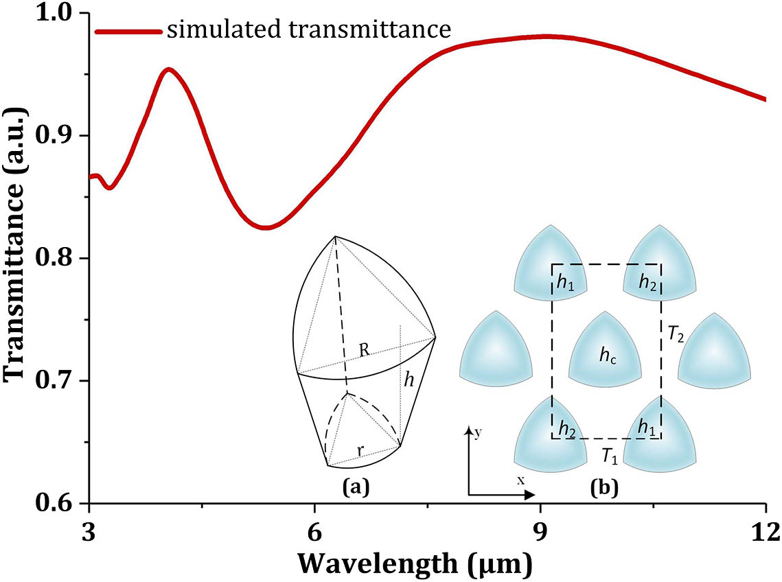
Fig. 1. Optimal simulated transmittance (red line) of the Reuleaux-triangle-shaped hole array on Ge for T1=1.1μm, R=1μm, and r=0.8μm. Inset (a) is a single Reuleaux-triangle-shaped hole, and (b) shows Reuleaux-triangle-shaped holes forming a closely packed hexagonal array (top view). The polarization direction of the incident light is 0° with the x axis.

下载图片 查看所有图片

The Reuleaux-triangle-shaped holes are closely packed into a hexagonal array, as shown in Fig. 1 inset (b). Five holes constitute one period of the array, which is represented by a rectangle with horizontal length T1 and vertical length T2.

Rigorous vector diffraction theory was used to simulate the transmittance of the Reuleaux-triangle-shaped hole array on one side of the Ge substrate, and the other side is ideal non-reflection. In general, the value of T1 should be less than the shortest wavelength of the target waveband. The closer R is to T1, the smaller the change in the refractive index from air to Ge is, and less reflection occurs. The effective index of the micro-nanostructure depends on the duty cycle[15]; when T1 is fixed, the value of α determines the value of the duty cycle. The steepness α determines the intensity and location of the peak transmittance. Considering the machining accuracy, we fix T1 as 1.1 μm and R as 1 μm and vary r between 0.75 and 0.95 μm to simulate the transmittance at various α. The optimized result is shown in Fig. 1 (red line). The achieved optimal peak and average transmittances are 98.1% and 90.2%, respectively, at α=84°, which corresponds to r=0.8μm. Starting from the edge of the waveband at 3 μm, the transmittance declines until 3.27 μm, increases to reach a first peak at 4.08 μm (the central wavelength of the MWIR band), declines to its lowest point at 5.37 μm, before again increasing to a second peak at 9.67 μm (the central wavelength of the LWIR band), and then decreases slowly.

To explore the optical properties of the Reuleaux-triangle-shaped holes, we simulated the electric field distribution for a single period of the hole array [the rectangular region with the dashed outline in Fig. 1 inset (b)] via the finite-difference time-domain (FDTD) method. The results are shown in Fig. 2. When a 3–12 μm electromagnetic wave with uniform electric field [Fig. 2(a)] passes through these Reuleaux-triangle-shaped holes, the incident and reflected radiation will interfere at the vertices of the Reuleaux triangles, where their electric field intensities will be enhanced [see the orange and red areas in Figs. 2(b)(h)]. Comparing the transmittance in Fig. 1 and the electric field intensity in Fig. 2, we find a distinct correspondence between them. The change in electric field intensity with wavelength (Fig. 2) is consistent with the spectral transmittance plot (Fig. 1). At the peak wavelengths of the transmittance, 4.08 μm (the central wavelength of the MWIR band) and 9.67 μm (the central wavelength of the LWIR band), the electric field intensities also reach peak values.
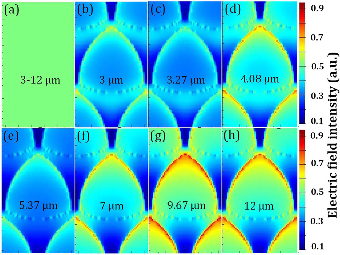
Fig. 2. Electric field distributions for a single period of the Reuleaux-triangle-shaped hole array: (a) incident 3–12 μm electromagnetic wave with uniform distribution of field intensity, and (b)–(h) different mid-IR wavelengths passing through the Reuleaux-triangle-shaped holes. The incident light is TE polarized.

下载图片 查看所有图片

When fabricating the Reuleaux-triangle-shaped hole array on Ge, large-area replication, sufficient hole depth, and the shape of Reuleaux triangle were the principal considerations. Nanoimprint lithography (NIL) and inductively coupled plasma (ICP) etching were selected for the fabrication in this work. NIL is an effective large-area nano-pattern replication technology that also possesses the advantages of ultra-high resolution, high output, and low cost. ICP technology can achieve sufficient depth and steepness with appropriate proportions of etchant, passivator, and physical bombardment gas. In addition, inspired by the fact that a disorderly distribution of triangles will form on the {111} planes of cubic crystals (Si, Ge) by chemical etching[16] and induction annealing[17], we attempted to fabricate an orderly Reuleaux-triangle-shaped hole array on {111} Ge with a simple circular mold.

A double-side-polished, N-type Ge wafer (540Ω·cm, 25.4 mm diameter, {111} cut) was used as the substrate. First, it was coated with photoresist (04n, Obducat AB, Sweden). Then, the circular patterns of the circular mold were transferred to the photoresist by NIL; the imprinting temperature, pressure, and time were 70°C, 40 bar, and 120 s, respectively. The Ge substrate was etched in a BCl3/Cl2/Ar atmosphere for 22 min with an ICP power of 100 W and a bias power of 30 W. In this process, Cl2 is the main etchant that reacts with Ge, producing nonvolatile GeCl4. The reaction equation is Ge+2Cl2=GeCl4.

The rate of etching is mainly determined by the chemical reaction between Cl2 and Ge. During the etching process, BCl3 acts as a passivator for the Ge surface. It is probably ionized into B–Cl and Cl[18]. The reaction equation is BCl3=BCl+2Cl.

B–Cl adheres to the Ge surface to prevent further reaction between Cl2 and Ge. Cl also reacts with Ge, but to a much less extent than Cl2. The influence of the BCl3 flow rate on the etching rate is slight, but sufficiently significant to form a ramp sidewall[19], which yields the gradient-index layer. The higher the BCl3 flow rate, the less steep the ramp. In our work, the Cl2/BCl3 gas ratio was optimized to be 30/20. The use of Ar allows removal of the main product of the reaction between Cl2 and Ge—nonvolatile GeCl4—by physical bombardment. The Ar flow rate increases 5 sccm every 7 min, from 25 sccm to 35 sccm, to achieve a hole depth of 1.1 μm. After etching, the Ge substrate was immersed in acetone for 2 h to remove the residual photoresist. Finally, a large area of gradient-index Reuleaux-triangle-shaped hole array on a Ge wafer was achieved [as shown in Fig. 3(a)].
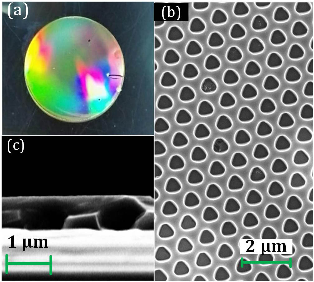
Fig. 3. (a) Photograph and (b) SEM micrograph of the fabricated Ge wafer with a Reuleaux-triangle hole array. (c) SEM side view of two Reuleaux-triangle holes.

下载图片 查看所有图片

Figure 3(b) shows the scanning electron microscope (SEM) micrograph of the fabricated Reuleaux-triangle hole array. With the help of the circular mold, an orderly and periodically distributed Reuleaux-triangle-shaped hole array was successfully prepared. T1 and T2 were measured to be approximately 1.1 and 1.9 μm, respectively. Figure 3(c) shows a side view of two Reuleaux-triangle holes. The depth h, as shown in the figure, is about 0.9 μm, which is smaller than the designed value. The slanted sidewall, which forms the gradient index for broadband antireflection, is clearly apparent in Fig. 3(c). R and r are around 1 and 0.8 μm, respectively, and calculated α is approximately 83°, slightly smaller than the theoretical optimal value of 84°.

Transmittance of the fabricated element at the normal incidence angle was measured using a double-beam IR spectrometer (WGH-30, Tianjin Gangdong Sci. & Tech. Development Co., Ltd.). Figure 4(a) shows the measured transmission spectra (yellow line); the transmittance of a Ge substrate with thickness of 2 mm (blue line) and the maximum theoretical antireflection on one side (red line) are also shown for comparison. It should be noted that the gradient-index Reuleaux-triangle-shaped hole array on Ge improves the transmittance, compared to the bare Ge surface, throughout the entire waveband from 3 to 12 μm: the average transmittance increases by 15.67%, from 45.82% to 61.49%. The transmittance decreases at the edge of the shortwave band due to diffraction. Incident-angle-dependent transmission is important for large field of view detection. Figure 4(b) shows that the transmittances maintain stability at the incidence angle of up to 60°.
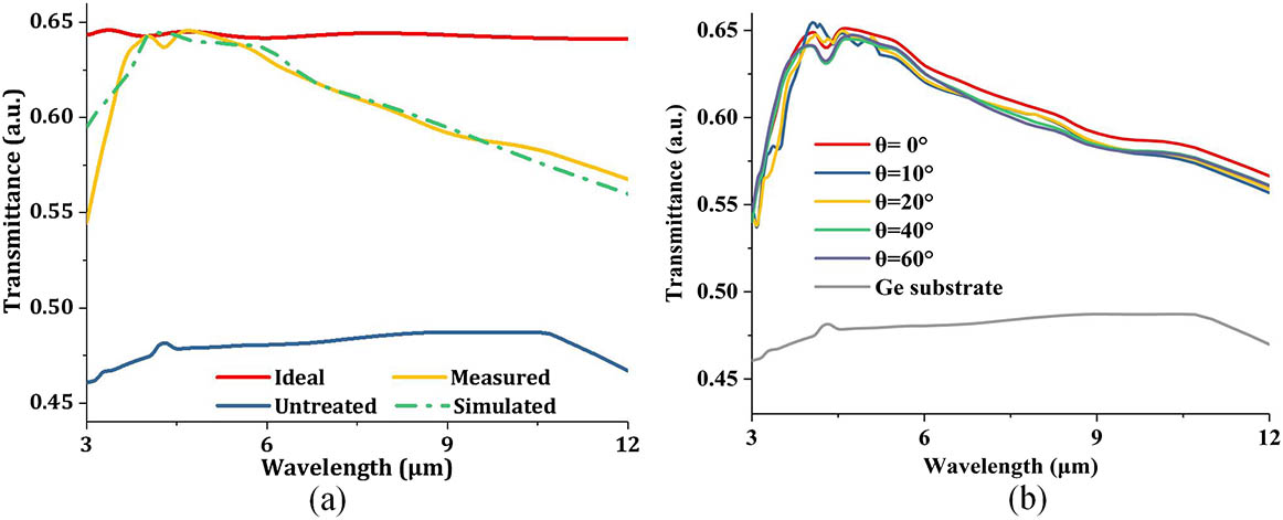
Fig. 4. (a) Transmission spectra of the fabricated element (yellow line), Ge substrate (2 mm thickness, blue line), updated simulated element with nonuniform hole depths (green dot-dashed line), and the maximum theoretical antireflection on one side (red line). (b) The measured transmittance versus incident angle.

下载图片 查看所有图片

In addition, we noticed that the measured transmission curve in Fig. 4 exhibits a shape that is different to that of the simulation in Fig. 1. Further investigations revealed that the fabricated Reuleaux-triangle holes practically possess nonuniform hole depths. The updated simulated transmission curve of a single period of holes with nonuniform depths is consistent with the measured one, as shown in Fig. 4(a). The hole depths are hc=0.8μm, h1=0.6μm, and h2=1.4μm [hc, h1, and h2 are defined in Fig. 1 inset (b)]. This result signifies that the etching of the Ge {111} plane is a process where triangular pyramids appear and disappear, and finally form the rugged bottom of the Reuleaux-triangle-shaped hole. It is caused by the arrangement of atoms in different orientations of the material itself. We can conclude, therefore, that nonuniform hole depths can modulate the transmittance over the 3–12 μm waveband.

In summary, we successfully fabricated a large-area gradient-index Reuleaux-triangle-shaped hole array on the Ge {111} plane by NIL and ICP etching to realize a broadband mid-IR AR surface. The average transmittance increases 15.67% over the waveband at 3–12 μm and maintains stability at the incidence angle of up to 60°. At the vertices of the Reuleaux triangle, the electric field intensities are enhanced due to interference of the incident and reflected radiation. This local enhancement characteristic is probably also useful for the development of mid-IR radiation-trapping micro-nanostructures for IR detectors. We were also able to establish that nonuniform hole depths can modulate the shape of the transmittance curve. In the future, we will further investigate the effect of nonuniform hole depths or nonuniform diameters on the modulation of the properties of IR optical materials.

References

[1] BusseL. E.FrantzJ. A.ShawL. B.AggarwalI. D.SangheraJ. S., Appl. Opt.54, F303 (2015).APOPAI0003-6935

[2] BusseL. E.FloreaC. M.FrantzJ. A.ShawL. B.AggarwalI. D.PoutousM. K.JoshiR.SangheraJ. S., Opt. Mater. Express4, 2504 (2014).

[3] DiaoZ.KrausM.BrunnerR.DirksJ.-H.SpatzJ. P., Nano Lett.16, 6610 (2016).NALEFD1530-6984

[4] KryuchkovM.LehmannJ.SchaabJ.CherepanovV.BlagodatskiA.FiebigM.KatanaevV. L., J. Nanobiotechnol.15, 61 (2017).

[5] PratesiF.BurresiM.RiboliF.VynckK.WiersmaD. S., Opt. Express21, A460 (2013).OPEXFF1094-4087

[6] SunC.-H.HoB. J.JiangB.JiangP., Opt. Lett.33, 2224 (2008).OPLEDP0146-9592

[7] DaglarB.KhudiyevT.DemirelG. B.BuyukserinF.BayindirM., J. Mater. Chem. C1, 7842 (2013).

[8] SongY. M.BaeS. Y.YuJ. S.LeeY. T., Opt. Lett.34, 1702 (2009).OPLEDP0146-9592

[9] GeL.WangX.ChenH.QiuK.FuS., Chin. Opt. Lett.10, 090502 (2012).

[10] NgC. H. B.FanW. Y., J. Am. Chem. Soc.136, 12840 (2014).JACSAT0002-7863

[11] WangK.ChenZ.-L.ZouH.-H.HuK.LiH.-Y.ZhangZ.SunW.-Y.LiangF.-P., Chem. Commun.52, 8297 (2016).

[12] WebsterA., Mon. Not. R. Astron. Soc.353, 1304 (2004).MNRAA40035-8711

[13] ZartilasS.PapatriantafyllopoulouC.StamatatosT. C.NastopoulosV.CremadesE.RuizE.ChristouG.LampropoulosC.TasiopoulosA., Inorg. Chem.52, 12070 (2013).INOCAJ0020-1669

[14] NgC. H. B.FanW. Y., ChemNanoMat2, 133 (2016).

[15] LawrenceR., Chen. Chin. Opt. Lett.15, 010004 (2017).

[16] PersichettiaL.FanfoniM.De SetaM.Di GaspareaL.OttavianocL.GolettiC.SgarlataA., Appl. Surf. Sci.462, 86 (2018).ASUSEE0169-4332

[17] Wright JenkinsM., J. Electrochem. Soc.124, 757 (1977).JESOAN0013-4651

[18] KimT. S.YangH. Y.ChoiS. S.JeongT. S.KangS.ShimK. H., Electron. Mater. Lett.5, 43 (2009).

[19] OehrleinG. S.RembetskiJ. F.PayneE. H., J. Vac. Sci. Technol. B: Microelectron. Process. Phenom.8, 1199 (1990).

Haijuan Cheng, Miao Dong, Qinwen Tan, Linghai Meng, Yi Cai, Jie Jiang, Weisheng Yang, Haizheng Zhong, Lingxue Wang. Broadband mid-IR antireflective Reuleaux-triangle-shaped hole array on germanium[J]. Chinese Optics Letters, 2019, 17(12): 122401.


本文已被 4 篇论文引用
被引统计数据来源于中国光学期刊网
引用该论文: TXT   |   EndNote

相关论文

加载中...

关于本站 Cookie 的使用提示

中国光学期刊网使用基于 cookie 的技术来更好地为您提供各项服务,点击此处了解我们的隐私策略。 如您需继续使用本网站,请您授权我们使用本地 cookie 来保存部分信息。
全站搜索
您最值得信赖的光电行业旗舰网络服务平台!