1 中国科学院上海光学精密机械研究所信息光学与光电技术实验室, 上海 201800
2 中国科学院大学材料与光电研究中心, 北京 100049
基于共振域光栅的特性,采用商用绝缘硅片设计并制备了一种用于近红外通信波段的高性能偏振器件。在1.460~1.625μm的波长范围内,利用时域有限差分算法设计了一种周期为0.98μm的全介质共振域光栅,该光栅的消光比最大值为55dB。根据设计结果,采用电子束直写曝光技术对该偏振光栅进行了实验制备,并进行偏振性能测试。结果表明,该光栅的横向磁场偏振光透过率约在80%以上,消光比在20dB以上,最大值可达到32dB,与仿真结果基本一致。相比于传统亚波长金属光栅的周期需要小于1/4入射光波长才能起偏的性质,该偏振光栅在周期为近波长的条件下即有较好的偏振性能,在制备上降低了光刻工艺的难度。此外,该偏振器件是基于商用绝缘硅片制备,与现有的成熟半导体工艺兼容,具有较强的集成性和实用性。
光学器件 偏振器 绝缘硅片 共振域光栅 透过率 消光比 中国激光
2020, 47(12): 1201005
Author Affiliations
Abstract
1 Image Processing Systems Institute—Branch of the Federal Scientific Research Centre “Crystallography and Photonics” of Russian Academy of Sciences, 151 Molodogvardeyskaya St., Samara 443001, Russia
2 Samara National Research University, 34 Moskovskoe Shosse, Samara 443086, Russia
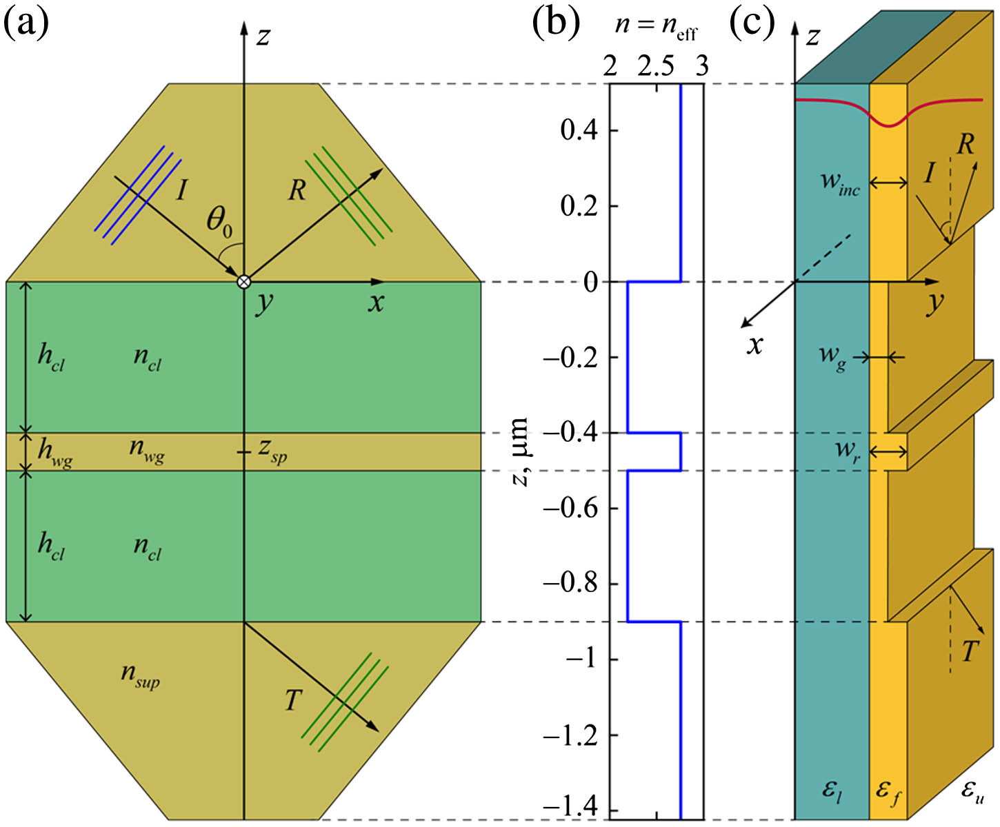
We propose a simple integrated narrowband filter consisting of two grooves on the surface of a slab waveguide. Spectral filtering is performed in transmission at oblique incidence due to excitation of an eigenmode of the structure localized at a ridge cavity between the grooves. For the considered parameters, zero reflectance and unity transmittance are achieved at resonant conditions. The width and location of the transmittance peak can be controlled by changing the widths of the grooves and of the ridge, respectively. The proposed filter may find application in waveguide-integrated spectrometers.
Wavelength filtering devices Microcavity devices Integrated optics devices Guided waves Resonance domain Subwavelength structures Photonics Research
2018, 6(1): 01000061
重庆文理学院 电子电气工程学院, 信息光电子技术与应用研究所, 重庆 402160
采用模态法研究了共振域光栅分束器及闪耀光栅等光学器件的设计原理及逆向设计方法, 给出了-1级非偏振闪耀光栅的典型设计示例。研究表明, 自准直角入射时, 光束在光栅内传输将激发产生离散模, 通过调节离散模透过光栅传输时的累积相位差, 可对衍射光进行调控, 实现偏振(非偏振)分束、偏振(非偏振)闪耀等功能。采用严格耦合波法对基于模态法逆向设计的-1级非偏振石英闪耀光栅的几何参数进行验证, 计算结果显示两者非常吻合, 证明了该方法的正确性。
闪耀光栅 模态法 共振域 逆向设计 blazed grating modal method resonance-domain reverse design
Author Affiliations
Abstract
State Key Laboratory on Integrated Optoelectronics, Institute of Semiconductors, Chinese Academy of Sciences, Beijing 100083, China
The effect of shape, height, and interparticle spacing of Au nanoparticles (NPs) on the sensing performance of Au NP array is systematically investigated. Lengthening the major axis of elliptical NPs with the minor axis kept constant will cause the redshift of the local surface plasmon (LSP) resonance mode, enhance the sensitivity, and widen the resonance peaks. Larger height corresponds to smaller LSP resonance wavelength and narrower resonance peak. With each NP size unchanged, larger interparticle spacing corresponds to larger resonance wavelength and smaller full-width at half-maximum (FWHM). Moreover, duty cycle is important for sensitivity, which is largest when the duty cycle is 0.4.
灵敏度 半高宽 共振波长 纳米颗粒阵列 050.5745 Resonance domain 240.6680 Surface plasmons 120.7000 Transmission Chinese Optics Letters
2011, 9(9): 090501
Author Affiliations
Abstract
Department of Electrooptic Engineering, Ben Gurion University of the Negev, Beer Sheva 84105, Israel
Applicability of guided mode resonant structures to tunable optical filtering and sensing is demonstrated using nematic liquid crystals. As a sensor, a minimum refractive index detectivity of 10^{-5} is demonstrated while as a tunable filter, tunability range of few tens of nanometers with 2-nm bandwidth is presented. The optimum design is achieved by maximizing the evanescent field region in the analyte which maximizes the overlap integral. The device can be operated in reflection or transmission modes at normal incidence. It can also be operated at a single wavelength by measuring the angular profile of the light beam.
波导管共振 光学传感器 可调滤光片 液晶 050.5745 Resonance domain 050.6624 Subwavelength structures 130.2790 Guided waves 230.3720 Liquid-crystal devices Chinese Optics Letters
2009, 7(8): 08667


