郑州大学电气与信息工程学院河南省激光与光电信息技术重点实验室,河南 郑州 450001
二维光子Moiré超晶格拥有一些常规光子晶体不具备的特性,例如平带特征和不同于安德森局域化的光局域现象。本文利用多光束干涉法构建二维光子Moiré超晶格结构,采用有限元法对其能带结构及光场特性进行研究。通过优化Moiré晶格厚度、空气孔半径对其平带及局域特性的影响,得到了高局域特性的Moiré晶格结构。研究中发现,正方晶格具有不同于六角晶格的准狄拉克锥光局域化效应。本文研究结果对发展高性能微纳结构器件具有重要参考价值。
光子晶体 光子Moiré超晶格 多光束干涉 平带 光局域
1 中国科学院半导体研究所, 北京 100083
2 中国电子科技集团公司第四十一研究所, 山东青岛 266555
光电导天线作为太赫兹时域光谱仪产生与探测太赫兹辐射的关键部件, 具有重要的科研与工业价值。本文采用分子束外延 (MBE)方法制备 InGaAs/InAlAs超晶格作为 1 550 nm光电导天线的光吸收材料, 使用原子力显微镜、光致发光、高分辨 X射线衍射等方式验证了材料的高生长质量; 通过优化制备条件得到了侧面平整的台面结构光电导天线。制备的光电导太赫兹发射天线在太赫兹时域光谱系统中实现了 4.5 THz的频谱宽度, 动态范围为 45 dB。
太赫兹时域光谱仪 光电导天线 分子束外延 InGaAs/InAlAs超晶格 terahertz time-domain spectrometer photoconductive antenna Molecular Beam Epitaxy InGaAs/InAlAs superlattices 太赫兹科学与电子信息学报
2023, 21(12): 1403
1 昆明理工大学 理学院,云南 昆明 650091
2 云南大学 物理与天文学院,云南 昆明 650091
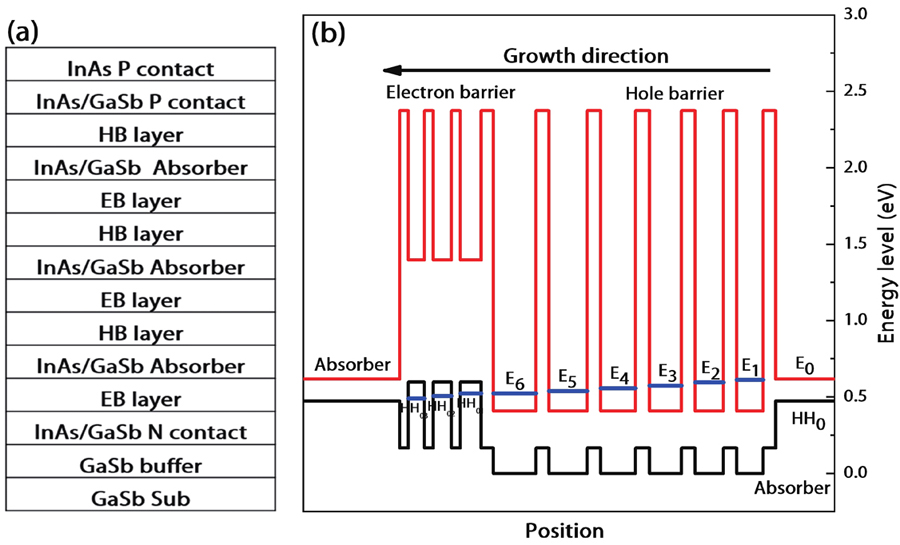
本文系统报道了基于InAs/GaSb Ⅱ类超晶格(T2SLs)的长波红外探测器的研究进展。从衬底、材料生长以及器件性能角度对比分析了基于GaSb、InAs 衬底的各种器件结构的优缺点。分析结果表明,以InAs 为衬底、吸收区材料为InAs/InAs1-xSbx、PB1IB2N 型的结构为相对优化的器件结构设计,结合ZnS 和Ge 的多层膜结构设计或者重掺杂缓冲层,同时采用电感耦合等离子体(inductively coupled plasma)干法刻蚀工艺,该器件的50%截止波长可达12 ?m,量子效率(quantum efficiency)可提升到65%以上,暗电流密度降低至1×10⁻⁵ A/cm2。并归纳总结了InAs/GaSb T2SLs 长波红外探测器未来的发展趋势。
InAs/GaSbⅡ类超晶格 器件结构 暗电流 量子效率 结构优化 InAs/GaSb type-II superlattices, device structure,
1 北京邮电大学 信息光子学与光通信全国重点实验室,北京 100876
2 超晶科技(北京)有限公司,北京 100083
3 西南技术物理研究所,成都 610041
4 电子科技大学 基础与前沿研究院,成都 610054
二类超晶格(T2SL)相对于其它制冷型红外探测器材料体系,具有成本低、均匀性高、工艺兼容性好等特点,且波长灵活可调、俄歇复合速率低。k·p方法作为一种常用且相对成熟的能带结构仿真技术,具有计算精度高、节省计算资源等特点,在T2SL的仿真中受到了广泛的关注。梳理了中波、长波、甚长波T2SL红外探测器的仿真进展,归纳了k·p方法的发展过程,以及该方法在T2SL红外探测器仿真中的进展和作用,直观展示k·p方法在超晶格仿真工作中的准确性与便利性; 重点讨论了T2SL探测器的暗电流机制、量子效率和吸收光谱等性质,对T2SL红外探测器的研究和应用前景进行展望。采用包络函数近似下的k·p方法可以对超晶格材料的能带结构和电子性质进行较为准确的理论分析和仿真计算。
探测器 二类超晶格 k·p方法 器件仿真 detectors type-Ⅱ superlattices the k·p method device simulation
光子学报
2023, 52(10): 1052405
Author Affiliations
Abstract
1 The Key Laboratory of Semiconductor Materials Science, Institute of Semiconductors, Chinese Academy of Sciences, Beijing 100083, China
2 Center of Materials Science and Optoelectronics Engineering, University of Chinese Academy of Sciences, Beijing 100049, China
We report on a long wavelength interband cascade photodetector with type II InAs/GaSb superlattice absorber. The device is a three-stage interband cascade structure. At 77 K, the 50% cutoff wavelength of the detector is 8.48 μm and the peak photoresponse wavelength is 7.78 μm. The peak responsivity is 0.93 A/W and the detectivity D* is 1.12 × 1011 cm·Hz0.5/W for 7.78 μm at –0.20 V. The detector can operate up to about 260 K. At 260 K, the 50% cutoff wavelength is 11.52 μm, the peak responsivity is 0.78 A/W and the D* is 5.02 × 108 cm·Hz0.5/W for the peak wavelength of 10.39 μm at –2.75 V. The dark current of the device is dominated by the diffusion current under both a small bias voltage of –0.2 V and a large one of –2.75 V for the temperature range of 120 to 260 K.We report on a long wavelength interband cascade photodetector with type II InAs/GaSb superlattice absorber. The device is a three-stage interband cascade structure. At 77 K, the 50% cutoff wavelength of the detector is 8.48 μm and the peak photoresponse wavelength is 7.78 μm. The peak responsivity is 0.93 A/W and the detectivity D* is 1.12 × 1011 cm·Hz0.5/W for 7.78 μm at –0.20 V. The detector can operate up to about 260 K. At 260 K, the 50% cutoff wavelength is 11.52 μm, the peak responsivity is 0.78 A/W and the D* is 5.02 × 108 cm·Hz0.5/W for the peak wavelength of 10.39 μm at –2.75 V. The dark current of the device is dominated by the diffusion current under both a small bias voltage of –0.2 V and a large one of –2.75 V for the temperature range of 120 to 260 K.
interband cascade infrared photodetector type II superlattices long wavelength Journal of Semiconductors
2023, 44(4): 042301
Author Affiliations
Abstract
1 Advanced Research Institute of Multidisciplinary Science, Beijing Institute of Technology, Beijing 100081, China
2 Beijing National Laboratory for Condensed Matter Physics, Institute of Physics, Chinese Academy of Sciences, Beijing 100190, China
3 School of Physical Sciences, University of Chinese Academy of Sciences, Beijing 100049, China
4 School of Integrated Circuits and Electronics, MIIT Key Laboratory for Low-Dimensional Quantum Structure and Devices, Beijing Institute of Technology, Beijing 100081, China
5 BIT Chongqing Institute of Microelectronics and Microsystems, Chongqing 401332, China
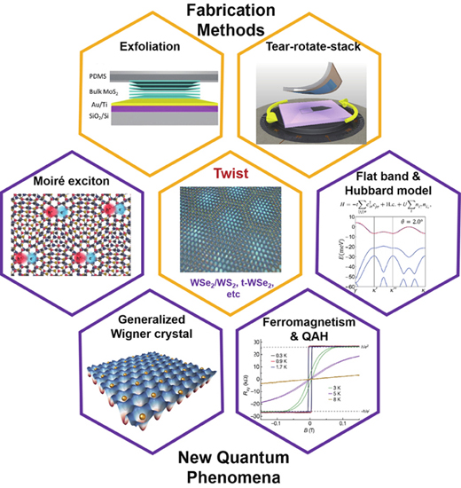
Moiré superlattices are formed when overlaying two materials with a slight mismatch in twist angle or lattice constant. They provide a novel platform for the study of strong electronic correlations and non-trivial band topology, where emergent phenomena such as correlated insulating states, unconventional superconductivity, and quantum anomalous Hall effect are discovered. In this review, we focus on the semiconducting transition metal dichalcogenides (TMDs) based moiré systems that host intriguing flat-band physics. We first review the exfoliation methods of two-dimensional materials and the fabrication technique of their moiré structures. Secondly, we overview the progress of the optically excited moiré excitons, which render the main discovery in the early experiments on TMD moiré systems. We then introduce the formation mechanism of flat bands and their potential in the quantum simulation of the Hubbard model with tunable doping, degeneracies, and correlation strength. Finally, we briefly discuss the challenges and future perspectives of this field.Moiré superlattices are formed when overlaying two materials with a slight mismatch in twist angle or lattice constant. They provide a novel platform for the study of strong electronic correlations and non-trivial band topology, where emergent phenomena such as correlated insulating states, unconventional superconductivity, and quantum anomalous Hall effect are discovered. In this review, we focus on the semiconducting transition metal dichalcogenides (TMDs) based moiré systems that host intriguing flat-band physics. We first review the exfoliation methods of two-dimensional materials and the fabrication technique of their moiré structures. Secondly, we overview the progress of the optically excited moiré excitons, which render the main discovery in the early experiments on TMD moiré systems. We then introduce the formation mechanism of flat bands and their potential in the quantum simulation of the Hubbard model with tunable doping, degeneracies, and correlation strength. Finally, we briefly discuss the challenges and future perspectives of this field.
flat-band physics two-dimensional materials moiré superlattices Hubbard model moiré excitons Journal of Semiconductors
2023, 44(1): 011901
1 中国科学院上海技术物理研究所 红外成像材料与器件重点实验室,上海 200083
2 上海科技大学 信息学院,上海 201210
本文基于长波InAs / GaSb II类超晶格红外焦平面阵列(Focal Plane Array,FPA)设计和生长了由ZnS和Ge组成的多层薄膜结构。与没有多层薄膜的FPA相比,多层薄膜使其响应峰位置从8.7 μm和10.3 μm分别移动到9.8 μm和11.7 μm,50%响应截止波长从11.6 μm移动至12.3 μm,并且在波长为12 μm处的响应强度增加了69%。总之,优化的多层薄膜可以调控FPA的响应波长,这为实现更高灵敏度和更高成像能力的长波红外探测提供了更好的平台。
II类超晶格 焦平面阵列 多层薄膜 响应调控 Type-II superlattices FPAs multi-coatings tunable response


