1 深圳技术大学中德智能制造学院,广东 深圳 518118
2 温州大学机电工程学院,浙江 温州 325200
3 浙江大学机械工程学院,流体动力与机电系统国家重点实验室,浙江 杭州 310027
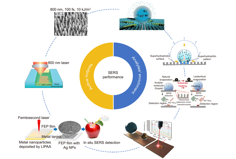
Overview: Surface-enhanced Raman scattering (SERS) affords a rapid, highly sensitive, and nondestructive approach for label-free and fingerprint diagnosis of a wide range of chemicals. This technique has been applied in explosives detection, pre-cancer diagnosis, food safety, and forensic analysis, where a small number of hazardous substances can seriously affect health of human beings. Thus, it is of great significance to prepare high-performance SERS sensors. In general, the signal intensity of SERS is determined by the following three factors: 1) The enhancement effect of surface nanostructure on local electric fields; 2) The number of molecules to be detected in hot spots; 3) Performance of the Raman spectrometer. Therefore, in order to achieve high-performance SERS detection of trace molecules, current research focuses on how to increase the density of hot spots and the number of analyte molecules in the detection area. An ultrafast laser has an ultra-short pulse width and ultra-high peak power, so it can interact with the majority of materials with high processing accuracy and excellent controllability. Meanwhile, it can rapidly construct a variety of large-area micro/nano-structures on material surfaces based on facile digital programming strategies. In addition, combined with multi-beam parallel fast scanning technology, low-cost and high-efficiency machining can be realized without a special requirement for the machining environment. Based on the above advantages, the ultrafast laser has become one of the important means for the fabrication of micro/nano-structures. This is important for the commercial preparation of high-performance SERS sensors. In this paper, we focus on two aspects to introduce the ultrafast laser preparation of high-performance SERS sensors, including how to increase the density of hot spots and the number of analyte molecules in the detection region. Ultrafast lasers can prepare micro/nano-structures with local field enhancement effects by both "bottom-up" and "top-down" processing strategies. The first is based on the "bottom-up" principle, where the reduction, deposition or polymerization of atoms, molecules or other nanoparticles is controlled by ultrafast lasers to achieve additive manufacturing of micro/nano-structures. The other is based on the "top-down" principle, where materials are removed by the ultrafast laser ablation to rapidly achieve hierarchical micro/nanostructures. These structures provide abundant active hot spots for SERS detection. In particular, the superhydrophobic surfaces prepared by the ultrafast laser are one of the most effective methods to achieve the enrichment of analyte molecules. Raman scattering can be excited more effectively by enriched molecules, which is conducive to obtaining higher detection limits and realizing ultra-trace detection. Finally, a prospect for the development of laser-prepared SERS substrates is provided.
超快激光加工 拉曼光谱 表面增强拉曼散射 微纳结构 ultrafast laser fabrication Raman spectroscopy surface-enhanced Raman scattering micro/nano-structures 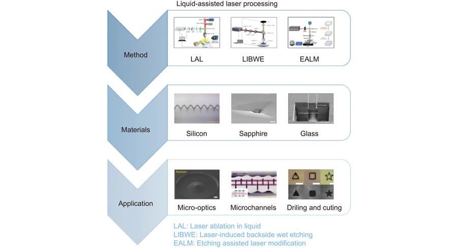
吉林大学电子科学与工程学院,集成光电子学国家重点实验室,吉林 长春 130012
Overview: With the development of industry, laser fabrication has become one of the important technologies for welding, cutting, surface processing, and other advanced manufacturing areas. At the same time, the pursuit of structures miniaturization, devices integration, and high precision has put forward more stringent requirements for laser fabrication technologies. Due to the advantages of stable mechanical and chemical properties and unique photoelectric properties, hard and brittle materials have been widely used in aerospace, the photoelectric industry, et al. Laser fabrication is an ideal technology for hard and brittle materials processing due to its high precision, high energy, and non-contact properties. In order to achieve the removal of hard and brittle materials, high laser energy is usually required, resulting in low fabrication accuracy and poor surface quality. As an improved laser processing method, liquidassisted laser fabrication can effectively improve fabrication accuracy and surface quality. The processing characteristics and material removal principles of three different liquid-assisted laser processing technologies are summarized in this review. According to the different functions of the medium through which the laser penetrates and the kinds of liquid, liquid-assisted laser fabrication technology can be divided into Laser ablation in liquid (LAL), laser-induced backside wet etching (LIBWE), and etching-assisted laser modification (EALM). The auxiliary liquid of Laser ablation in liquid is mostly water, which mainly plays the role of cooling and removing debris. The auxiliary liquids used by laser-induced backside wet etching include organic solvents, acid-base solutions, inorganic salts, and other liquids, which play different roles according to different liquids. The etching-assisted laser modification mainly uses an acid or alkaline solution as an auxiliary liquid to remove laser-modified materials. Different methods and auxiliary liquids have different mechanisms in the methods. Therefore, almost any material can be processed by choosing suitable methods and auxiliary liquids, including photosensitive glass, silicon crystal, sapphire, and other transparent hard brittle materials. Here, we summarize the fabrication technologies and fabrication parameters for different materials. The development and applications of liquid-assisted laser fabrication technologies in the fields of micro-optical components, microfluidic devices, and drilling and cutting are introduced. Finally, the challenges of the technology are discussed.
激光加工 硬脆材料 液体辅助制造 微/纳米结构 laser fabrication hard and brittle materials liquid assisted fabrication micro/nano structures
1 上海理工大学光电信息与计算机工程学院,上海 200093
2 中国科学院上海光学精密机械研究所薄膜光学实验室,上海 201800
高透过率的窗口材料是光电系统高精度和稳定性的重要保障。金刚石材料集优良的光学特性以及高热导率、低热膨胀系数等特性于一身,是性能优异的宽波段窗口材料。但金刚石在可见光及红外波段的高折射率限制了它的进一步应用,构筑减反射微纳结构抑制金刚石表面反射损耗是较为有效的方法之一。本文综述了近年来金刚石减反射微纳结构的研究进展,着重介绍了微纳结构的减反射机理以及激光加工和离子刻蚀两类加工方式的基本原理及工艺条件,总结了两种方式制备的表面微纳结构对金刚石透过率的影响,对比了各类制备技术的优缺点,并简单介绍了金刚石的应用前景,旨在为相关领域的研究人员提供技术参考。
表面光学 金刚石 微纳结构 减反射机理 激光加工 离子刻蚀 应用前景
1 School of Physics and Technology, Wuhan University, Wuhan 430072, Hubei , China
2 State Key Laboratory of Precision Spectroscopy, East China Normal University, Shanghai 200062, China
3 The Institute of Technological Sciences, Wuhan University, Wuhan 430072, Hubei , China
Gallium nitride (GaN) has widespread applications in the semiconductor industry because of its desirable optoelectronic properties. The fabrication of surface structures on GaN thin films can effectively modify their optical and electrical properties, providing additional degrees of freedom for controlling GaN-based devices. Compared with lithography-based techniques, laser processing is maskless and much more efficient. This paper shows how surface micro-nano structures can be produced on GaN thin films using 355 nm nanosecond laser irradiation. The effects of the laser pulse energy, number of pulses, and polarization direction were studied. It was found that distinct micro-nano structures were formed under different irradiation conditions, and their geometries and elemental compositions were analyzed. The results indicate that different types of surface micro-nano structures can be produced on GaN thin films in a controllable manner using 355 nm nanosecond laser irradiation. The results of our study provide valuable guidance for the surface modification of GaN-based optoelectronic devices.Gallium nitride (GaN) has widespread applications in the semiconductor industry because of its desirable optoelectronic properties. The fabrication of surface structures on GaN thin films can effectively modify their optical and electrical properties, providing additional degrees of freedom for controlling GaN-based devices. Compared with lithography-based techniques, laser processing is maskless and much more efficient. This paper shows how surface micro-nano structures can be produced on GaN thin films using 355 nm nanosecond laser irradiation. The effects of the laser pulse energy, number of pulses, and polarization direction were studied. It was found that distinct micro-nano structures were formed under different irradiation conditions, and their geometries and elemental compositions were analyzed. The results indicate that different types of surface micro-nano structures can be produced on GaN thin films in a controllable manner using 355 nm nanosecond laser irradiation. The results of our study provide valuable guidance for the surface modification of GaN-based optoelectronic devices.
gallium nitride thin films nanosecond laser micro-nano structures laser-induced periodic surface structures 激光与光电子学进展
2023, 60(7): 0714005
1 浙江大学现代光学仪器国家重点实验室, 浙江 杭州 310027
2 浙江大学光电科学与工程学院, 浙江 杭州 310027
3 浙江大学先进光子学国际研究中心, 浙江 杭州 310027
随着现代社会能源与极端气候问题日益严峻, 零能耗的辐射制冷技术越来越受到人们的关注与重视。从 2014 年日间辐射制冷首次被实验实现以来, 辐射制冷技术已从结构设计、材料选择、制备工艺、集成应用等多个角度被广泛研究, 产生了包括镀膜、涂层、柔性薄膜、织物等多种类型的器件。新的研究也越来越重视辐射制冷在场景兼容性以及环境、气候自适应性等方面的需求。开发多场景兼容、自适应环境变化且具有动态热调控能力的新型辐射制冷器件, 对辐射制冷技术的实用化以及能源、医疗、工业生产等领域都有着重要意义。本文围绕辐射制冷技术所运用的基础物理原理与光子学结构设计, 综述了辐射制冷器件的基本技术与其在场景兼容、温度自适应热调控等方面的进展。首先介绍了辐射制冷技术的原理与基本设计方法, 随后重点介绍了一些典型的辐射制冷结构以及实现多场景兼容与自适应动态调控辐射制冷器件的主要进展, 最后对辐射制冷器件的发展进行了总结与展望。
光学器件 辐射制冷 微纳结构 动态热调控 optical devices radiative cooling micro/nano structures dynamic thermal regulation
1 南京大学现代工程与应用科学学院,南京 210093
2 中国科学院材料力学行为与设计重点实验室,中国科学技术大学,合肥 230026
3 中国科学技术大学精密机械与仪器系,合肥 230026
4 南京大学人工微结构科学与技术协同创新中心,南京 210093
随着电子和能源科技的发展,基于纳米结构调控的新型热电材料以及热逻辑器件研究正受到越来越多的关注。本工作围绕几种具有应用潜力的热电材料,利用项目团队自主开发的微纳尺度热输运测试系统,从理论和实验上研究了原子及纳米尺度结构对热输运特性的调控机制,包括:全组分Si1-xGex合金薄膜的原子合金化,Bi2Ca2Co2Oy层状结构单晶的错配界面,超离子导体A0.5RhO2 (A=K, Rb, Cs)单晶的离子局域共振,准一维结构ZrTe5/HfTe5单晶中的疏松微结构,以及SnSe单晶中的SnSe2原子级插层,总结了不同尺度结构和原子间作用力对热传导性质的影响规律,为探索低热导率、高热电转换性能的新型热电材料提供有效的调控方案。最后,介绍了利用相变转换机制实现热导率高效动态调控的实验结果,及其在热逻辑器件方面的潜在应用。
热输运 热电材料 热逻辑器件 微纳结构 thermal transport thermoelectric materials thermal logic devices micro-nano structures
1 湖南大学材料科学与工程学院,长沙 410082
2 湖南立方新能源科技有限责任公司,湖南 株洲 412007
氟磷酸钒钠[Na3V2(PO4)2F3]凭借其高理论比容量、高能量密度、高输出电压和快速离子扩散能力,被认为是最具发展前景的高电压型钠离子电池正极材料之一。然而,其缓慢的电子传输动力学和电化学反应过程中易遭受较大的结构应力等不足,严重制约了其进一步发展。基于此,从合成方法、修饰改性策略(微纳结构构建、碳包覆、元素掺杂、电池组分优化)等方面系统综述了Na3V2(PO4)2F3最新研究进展并对其未来发展作了展望。
氟磷酸钒钠 合成方法 微纳结构设计 碳包覆 元素掺杂 电池组分优化 sodium vanadium fluorophosphate synthetic methods micro-nano structures fabrication carbon coating element doping battery composition optimization
1 清华大学机械工程系,北京 100084
2 摩擦学国家重点实验室,北京 100084
3 清华大学化学系,北京 100084
二氧化钛兼具优异的光化学性质和光学性质,被广泛应用于能源材料、光学信息等领域的微纳功能器件中。二氧化钛的微纳加工与成形技术是二氧化钛微纳功能器件制备的关键技术基础。超快激光由于具有超短脉宽和超高能量峰值等特性而成为理想的微纳制造工具之一,近年来在二氧化钛的微纳加工领域中得到了广泛的关注。综述了超快激光加工二氧化钛微纳结构及功能器件的研究进展,包括二氧化钛的性质及应用、超快激光与二氧化钛的作用机理、二氧化钛微纳结构的超快激光加工技术,介绍了利用这些技术加工的二氧化钛光解水制氢器件、图案化结构色器件和光学加密器件等微纳功能器件,并对超快激光微纳加工技术在二氧化钛微纳结构及功能器件加工领域中的应用前景进行了展望。
激光技术 二氧化钛 微纳结构 功能器件 超快激光 微纳制造 中国激光
2022, 49(22): 2200002


