针对光导开关高重复频率运行时产生丝电流加热, 使光导开关温度迅速超过材料最高允许使用温度, 造成开关失效或损伤的难题, 本文结合微通道散热技术和射流冷却技术的优点, 设计了射流微通道耦合高效散热器。通过实验测试, 对不同运行工况下射流微通道耦合高效散热器的传热特性进行了研究, 并与美国进口的蜂窝型微通道散热器进行散热性能对比。实验结果表明: 体积流量为 3 L/min的情况下, 射流微通道耦合高效散热器的换热系数超过 35 000 W/(K·m2), 散热量高达 1 000 W, 相比蜂窝型微通道散热器散热量提升了 45%。在测试流量下, 随着体积流量的增加, 射流微通道耦合高效散热器的平均换热系数接近线性增加, 而蜂窝型微通道散热器的平均换热系数在大流量下却增加缓慢。此外, 采用射流微通道耦合高效散热器冷却的热源面温度均匀性明显优于采用蜂窝型微通道散热器冷却的热源面温度均匀性, 采用射流微通道耦合高效散热器的热源面温度波动能降低 58%, 更有利于降低光导开关热应力。
射流阵列 微通道 实验研究 光导开关 jet array micro-channel experimental research Photoconductive Semiconductor Switches 太赫兹科学与电子信息学报
2023, 21(11): 1397
线性斯特林制冷机在整个工作过程中, 输入正弦交流电的频率精度是直接影响线性斯特林制冷机振动的重要因素。尤其是对于单活塞线性斯特林制冷机而言, 输入的正弦交流电频率精度将直接影响到与之相连的动力吸振器的减振性能。基于此, 本文在线性斯特林制冷机逆变器的研究基础上, 通过对 SPWM(Sinusoidal Pulse Width Modulation)波生成方法、逆变电路中 MCU(MoneyWise Credit Union)时钟频率及滤波电路中截止频率、电容和电感等多个参数的分析, 得到了开关数和频率精度之间的关系。根据实际应用的要求, 线性斯特林制冷机逆变器输出实际频率与目标频率误差不得超过 ±0.1Hz, 频率精度则需要求控制在± 0.1%以内。所以在该应用条件下, 本文在单片机 MCU频率为 72 MHz时找到了满足合适需求的开关次数在 1400~2400之间, 其对应的频率精度均小于±0.1%。
线性斯特林制冷机 开关数 截止频率 频率精度 linear Stirling refrigerator number of switches cut off frequency frequency accuracy
Chongqing United Microelectronics Center, Chongqing 401332, China
Frontiers of Optoelectronics
2022, 15(1): s12200
吉林大学 电子科学与工程学院 集成光电子学国家重点实验室, 长春 130012
聚合物平面光波导(PLC)器件以其低损耗、低成本、低功耗, 以及制备工艺简单等优点, 在光通信网络、微波光子学、传感监控等领域发挥着重要作用。文章梳理了近年来聚合物平面光波导器件的代表性工作, 其中包括阵列波导光栅、可变光衰减器、光开关及其集成器件, 讨论了聚合物平面光波导未来的发展方向。
聚合物 波导器件 集成光学 阵列波导光栅 光开关 polymer planar lightwave circuit integrated optics array waveguide grating optical switches
1 国防科技大学 a.前沿交叉学科学院,湖南长沙 410073
2 b.脉冲功率激光技术国家重点实验室,安徽合肥 230037
磁开关因其优异的特性而被广泛用于固态脉冲功率调制器中,基于磁开关的多脉冲发生器的同步运行对产生更高功率的脉冲具有重要意义。与其他高功率开关相比,磁开关存在一种基于磁耦合机制的被动同步技术。通过耦合线圈相连的磁开关能够被动地减少磁开关之间的抖动,使多个磁开关趋于同步运行。设计了一个两路磁开关同步运行实验,实验结果显示差异为2.2 μs和 0.3 μs的 2个脉冲在引入磁耦合之后差异分别降至 0.6 μs和 0.1 μs,表明该磁耦合技术能成倍减少两台装置的输出抖动。此外,还针对磁开关同步运行过程及磁耦合机制进行了合理分析,并开展了基于 PSpice的磁开关同步电路仿真研究,提出了一种改进型回转器 -电容等效电路模型,该电路模型能有效地重现实验结果,为更深入理解磁开关同步运行技术及分析磁耦合机制奠定了基础。
功率合成 磁开关同步 磁耦合 回转器 -电容模型 power combination synchronization of magnetic switches magnetic coupling gyrator -capacitor model 太赫兹科学与电子信息学报
2021, 19(1): 170
Wuhan National Laboratory for Optoelectronics, Huazhong University of Science and Technology, Wuhan 430074, China
Frontiers of Optoelectronics
2020, 13(2): 129
Author Affiliations
Abstract
1 Taiyuan Satellite Launch Center, Kelan 036300, China
2 College of Optoelectronic Science and Engineering, National University of Defense Technology, Changsha 410073, China
Synchronization for multiple-pulse at nanosecond range shows a great value on the power multiplication and synchronous electric fields applications. Nanosecond or sub-ns jitter synchronization is essential for the improved working efficiency of the large amounts of pulse modules and accurate requirements for the power coherent combining applications. This paper presents a trigger generator based on a laser diodetriggered GaAs photoconductive semiconductor switch (PCSS) with low jitter and compact size characteristics. It avoids the high currents that are harmful to high-gain mode PCSSs. In the trigger circuit, a 200 pF capacitor is charged by a microsecond-scale 18 kV pulse and then discharged via the high-gain mode GaAs PCSS to trigger the high-power trigatron switch. When triggered by the ~10 ns pulse generated by the PCSS, the DC-charged trigatron can operate in the 20e35 kV range with 10 ns rise time and 1 ns delay-time jitter.
Pulsed power High power switches Synchronization Trigger generator Photoconductive semiconductor switch Matter and Radiation at Extremes
2018, 3(5): 256
Author Affiliations
Abstract
1 State Key Laboratory on Integrated Optoelectronics, Institute of Semiconductors, Chinese Academy of Science, Beijing 100083, China
2 College of Materials Science and Opto-Electronic Technology, University of Chinese Academy of Sciences, Beijing 100083, China
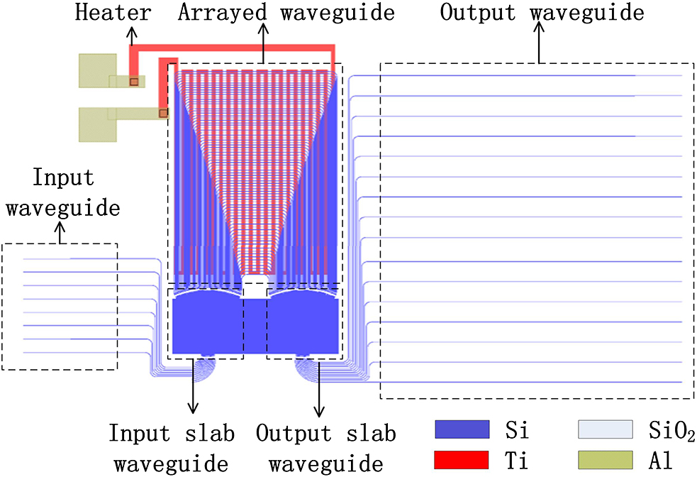
In this Letter, a 16 channel 200 GHz wavelength tunable arrayed waveguide grating (AWG) is designed and fabricated based on the silicon on insulator platform. Considering that the performance of the AWG, such as central wavelength and crosstalk, is sensitive to the dimension variation of waveguides, the error analysis of the AWG with width fluctuations is worked out using the transfer function method. A heater is designed to realize the wavelength tunability of the AWG based on the thermo-optic effect of silicon. The measured results show that the insertion loss of the AWG is about 6 dB, and the crosstalk is 7.5 dB. The wavelength tunability of 1.1 nm is achieved at 276 mW power consumption, and more wavelength shifts will gain at larger power consumption.
060.1810 Buffers, couplers, routers,switches, and multiplexers 060.4230 Multiplexing 230.7390 Waveguides, planar Chinese Optics Letters
2018, 16(1): 010601

Author Affiliations
Abstract
1 College of Science, Zhejiang University of Technology, Hangzhou 310023, China
2 Institute for Information Recording of NAS of Ukraine, Shpak Str. 2, Kiev 03113, Ukraine
We propose a design for efficient end-fire coupling of surface plasmon polaritons in a metal-insulator-metal (MIM) waveguide with an optical fiber as part of a simple photoplastic connector. The design was analyzed and optimized using the three-dimensional finite-difference time-domain method. The calculated excitation efficiency coefficient of the waveguide is 83.7% ( 0.77 dB) at a wavelength of 405 nm. This design enables simple connection of an optical fiber to a MIM waveguide and highly efficient local excitation of the waveguide. Moreover, the length of the metallic elements of the waveguide, and thus the dissipative losses, can be reduced. The proposed design may be useful in plasmonic-type waveguide applications such as near-field investigation of live cells and other objects with super-resolution.
Buffers, couplers, routers, switches, and multipl Near-field microscopy Plasmonics Photonics Research
2018, 6(3): 03000149
西北核技术研究所, 强脉冲辐射模拟与效应国家重点实验室, 西安 710024
目前MA级快脉冲直线变压器驱动源(FLTD)模块一般引入2~4路快前沿(约20 ns)高幅值(100 kV)电脉冲触发,百TW级数十MA的FLTD驱动源含有数千个模块,其触发系统非常庞大,并且要求触发脉冲按照精确时序到达各级串联模块,以便实现与次级行波同步的感应电压高效叠加,触发系统成为大型FLTD驱动源的瓶颈之一。在之前提出的一种利用一路外触发脉冲实现数十模块串联FLTD与次级行波同步的感应电压高效叠加触发方式基础上,设计了4级串联共用腔体的MA级FLTD模块组,每级共24支路,其中1个用作触发支路,主放电支路由2只100 nF双端引出电极电容器和1只GW级气体开关组成;建立了16级串联、次级为水线的单路FLTD电路模型,数值仿真研究了支路开关自放电、触发支路开关闭合时序与分散性,以及次级传输线阻抗对驱动源的影响。
快Z箍缩 FLTD驱动源 感应腔 GW级气体开关 同步触发 触发时序 fast Z-pinch fast linear transformer driver cavities GW gas spark switches triggering synchronization inductive voltage adder sequences 强激光与粒子束
2018, 30(3): 035001


