
Author Affiliations
Abstract
1 State Key Laboratory of Information Photonics and Optical Communications and School of Science, Beijing University of Posts and Telecommunications, Beijing 100876, China
2 School of Ethnic Minority Education, Beijing University of Posts and Telecommunications, Beijing 100876, China
The modulation of resonance features in microcavities is important to applications in nanophotonics. Based on the asymmetric whispering-gallery modes (WGMs) in a plasmonic resonator, we theoretically studied the mode evolution in an asymmetric WGM plasmonic system. Exploiting the gap or nano-scatter in the plasmonic ring cavity, the symmetry of the system will be broken and the standing wave in the cavity will be tunable. Based on this asymmetric structure, the output coupling rate between the two cavity modes can also be tuned. Moreover, the proposed method could further be applied for sensing and detecting the position of defects in a WGM system.
Microcavities Optical sensing and sensors Optical resonators Photonics Research
2017, 5(2): 02000113

Author Affiliations
Abstract
1 State Key Laboratory for Mesoscopic Physics and Department of Physics, Peking University, Beijing 100871, China
2 Research Institute for Electronic Science, Hokkaido University, Sapporo 001-0021, Japan
3 Department of Applied Chemistry, National Chiao Tung University, Hsinchu 30010, Taiwan
4 Collaborative Innovation Center of Quantum Matter, Beijing 100871, China
5 e-mail: misawa@es.hokudai.ac.jp
6 e-mail: qhgong@pku.edu.cn
We investigate the superposition properties of the dipole and quadrupole plasmon modes in the near field both experimentally, by using photoemission electron microscopy (PEEM), and theoretically. In particular, the asymmetric near-field distributions on gold (Au) nanodisks and nanoblocks under oblique incidence with different polarizations are investigated in detail. The results of PEEM measurements show that the evolutions of the asymmetric near-field distributions are different between the excitation with s-polarized and p-polarized light. The experimental results can be reproduced very well by numerical simulations and interpreted as the superposition of the dipole and quadrupole modes with the help of analytic calculations. Moreover, we hypothesize that the electrons collected by PEEM are mainly from the plasmonic hot spots located at the plane in the interface between the Au particles and the substrate in the PEEM experiments.
Surface plasmons Near-field microscopy Multiphoton processes Spectroscopy, multiphoton Ultrafast lasers Photonics Research
2017, 5(3): 03000187

Author Affiliations
Abstract
1 MOE Key Laboratory of Space Applied Physics and Chemistry, and Shaanxi Key Laboratory of Optical Information Technology, School of Science, Northwestern Polytechnical University, Xi’an 710072, China
2 e-mail: jlzhao@nwpu.edu.cn
We investigate the electrically controlled light propagation in the metal–dielectric–metal plasmonic waveguide with a sandwiched graphene monolayer. The theoretical and simulation results show that the propagation loss exhibits an obvious peak when the permittivity of graphene approaches an epsilon-near-zero point when adjusting the gate voltage on graphene. The analog of electromagnetically induced transparency (EIT) can be generated by introducing side-coupled stubs into the waveguide. Based on the EIT-like effect, the hybrid plasmonic waveguide with a length of only 1.5 μm can work as a modulator with an extinction ratio of ~15.8 dB, which is 2.3 times larger than the case without the stubs. The active modulation of surface plasmon polariton propagation can be further improved by tuning the carrier mobility of graphene. The graphene-supported plasmonic waveguide system could find applications for the nanoscale manipulation of light and chip-integrated modulation.
Surface plasmons Subwavelength structures, nanostructures Waveguides Integrated optics devices Photonics Research
2017, 5(3): 03000162

Author Affiliations
Abstract
Key Lab of All Optical Network and Advanced Telecommunication Network of Ministry of Education, Institute of Lightwave Technology, Beijing Jiaotong University, Beijing 100044, China
A high sensitivity D-shaped hole double-cladding fiber temperature sensor based on surface plasmon resonance (SPR) is designed and investigated by a full-vector finite element method. Within the D-shaped hole double-cladding fiber, the hollow D-section is coated with gold film and then injected in a high thermo-optic coefficient liquid to realize the high temperature sensitivity for the fiber SPR temperature sensor. The numerical simulation results show that the peaking loss of the D-shaped hole double-cladding fiber SPR is hugely influenced by the distance between the D-shaped hole and fiber core and by the thickness of the gold film, but the temperature sensitivity is almost insensitive to the above parameters. When the thermo-optic coefficient is 2.8×10 4/°C, the thickness of the gold film is 47 nm, and the distance between the D-shaped hole and fiber core is 5 μm, the temperature sensitivity of the D-shaped hole fiber SPR sensor can reach to 3.635 nm/°C.
Fiber optics sensors Surface plasmons Thermal effects Photonics Research
2017, 5(2): 02000103
Author Affiliations
Abstract
1 Department of Electrical Engineering, The Pennsylvania State University, University Park, Pennsylvania 16802, USA
2 School of Electronics and Information Engineering, Beihang University, Beijing 100191, China
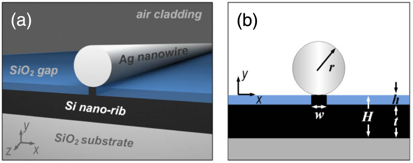
Hybrid plasmonic waveguides leveraging the coupling between dielectric modes and plasmon polaritons have emerged as a major focus of research attention during the past decade. A feasible way for constructing practical hybrid plasmonic structures is to integrate metallic configurations with silicon-on-insulator waveguiding platforms. Here we report a transformative high-performance silicon-based hybrid plasmonic waveguide that consists of a silicon nano-rib loaded with a metallic nanowire. A deep-subwavelength mode area (λ2/4.5×105 λ2/7×103), in conjunction with a reasonable propagation distance (2.2–60.2 μm), is achievable at a telecommunication wavelength of 1.55 μm. Such a nano-rib-based waveguide outperforms its conventional hybrid and plasmonic waveguiding counterparts, demonstrating tighter optical confinement for similar propagation distances and a significantly enhanced figure of merit. The guiding properties of the fundamental mode are also quite robust against possible fabrication imperfections. Due to the strong confinement capability, our proposed hybrid configuration features ultralow waveguide cross talk and enables submicron bends with moderate attenuation as well. The outstanding optical performance renders such waveguides as promising building blocks for ultracompact passive and active silicon-based integrated photonic components.
Guided waves Waveguides Surface plasmons Photonic integrated circuits Photonics Research
2018, 6(1): 01000037

Author Affiliations
Abstract
1 School of Electrical Engineering, Korea University, Anam-ro 145, Seongbuk-gu, Seoul 02841, South Korea
2 Department of Physics and KI for the NanoCentury, Korea Advanced Institute of Science and Technology, Daejeon 305-701, South Korea
We investigate the localized surface plasmon (LSP) effect by Al nanorings on the AlGaN/GaN multiple quantum well (MQW) structure emitting at 365 nm. For this experiment, first, the size of Al nanorings is optimized to maximize the energy transfer (or coupling) between the LSP and MQW using the silica nanospheres. Then, the Al nanorings with an outer diameter of 385 nm, which exhibit a strong absorption peak in the near-ultraviolet region, are applied to the top surface of the AlGaN/GaN MQW. The photoluminescence (PL) intensity of the MQW structure with Al nanorings increased by 227% at 365 nm compared to that without Al nanorings. This improvement is mainly attributed to an enhanced radiative recombination rate in the MQWs through the energy-matched LSPs by the temperature-dependent PL and time-resolved PL analyses. The radiative lifetime was about two times shorter than that of the structure without Al nanorings at room temperature. In addition, the measured PL efficiency at room temperature of the structure with Al nanorings was 33%, while that of the structure without Al nanorings was 19%, implying that LSP-QW coupling together with the nanoring array pattern itself played important roles in the enhancement.
Surface plasmons Light-emitting diodes Photoluminescence Photonics Research
2018, 6(1): 01000030
Author Affiliations
Abstract
1 Center for Terahertz Waves and College of Precision Instrument and Optoelectronics Engineering, Tianjin University, and the Key Laboratory of Optoelectronics Information and Technology Tianjin, Ministry of Education of China, Tianjin 300072, China
2 Physical Science and Engineering Division, King Abdullah University of Science and Technology, Thuwal 23955-6900, Saudi Arabia
3 School of Electrical and Computer Engineering, Oklahoma State University, Stillwater, Oklahoma 74078, USA
4 e-mail: weili.zhang@okstate.edu
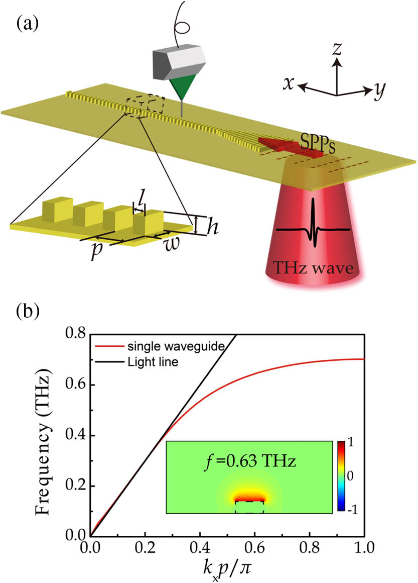
Surface plasmon polaritons (SPPs) with the features of subwavelength confinement and strong enhancements have sparked enormous interest. However, in the terahertz regime, due to the perfect conductivities of most metals, it is hard to realize the strong confinement of SPPs, even though the propagation loss could be sufficiently low. One main approach to circumvent this problem is to exploit spoof SPPs, which are expected to exhibit useful subwavelength confinement and relative low propagation loss at terahertz frequencies. Here we report the design, fabrication, and characterization of terahertz spoof SPP waveguides based on corrugated metal surfaces. The various waveguide components, including a straight waveguide, an S-bend waveguide, a Y-splitter, and a directional coupler, were experimentally demonstrated using scanning near-field terahertz microscopy. The proposed waveguide indeed enables propagation, bending, splitting, and coupling of terahertz SPPs and thus paves a new way for the development of flexible and compact plasmonic circuits operating at terahertz frequencies.
Integrated optics devices Surface waves Far infrared or terahertz Photonics Research
2018, 6(1): 01000018

Author Affiliations
Abstract
1 State Key Laboratory for Mesoscopic Physics, Collaborative Innovation Center of Quantum Matter, Department of Physics, Peking University, Beijing 100871, China
2 Collaborative Innovation Center of Extreme Optics, Shanxi University, Taiyuan 030006, China
The miniaturization of polarization beam splitters (PBSs) is vital for ultradense chip-scale photonic integrated circuits. However, the small PBSs based on complex hybrid plasmonic structures exhibit large fabrication difficulties or high insertion losses. Here, by designing a bending multimode plasmonic waveguide, an ultrabroadband on-chip plasmonic PBS with low insertion losses is numerically and experimentally realized. The multimode plasmonic waveguide, consisting of a metal strip with a V-shaped groove on the metal surface, supports the symmetric and antisymmetric surface plasmon polariton (SPP) waveguide modes in nature. Due to the different field confinements of the two SPP waveguide modes, which result in different bending losses, the two incident SPP waveguide modes of orthogonal polarization states are efficiently split in the bending multimode plasmonic waveguide. The numerical simulations show that the operation bandwidth of the proposed PBS is as large as 430 nm because there is no resonance or interference effect in the splitting process. Compared with the complex hybrid plasmonic structure, the simple bending multimode plasmonic waveguide is much easier to fabricate. In the experiment, a broadband (Δλ≈120 nm) and low-insertion-loss (<3 dB with a minimum insertion loss of 0.7 dB) PBS is demonstrated by using the strongly confined waveguide modes as the incident sources in the bending multimode plasmonic waveguide.
Beam splitters Polarization Surface plasmons Waveguides Photonics Research
2018, 6(1): 01000047

Author Affiliations
Abstract
1 School of Physics and Technology, University of Jinan, Jinan 250022, China
2 e-mail: sps_xiaw@ujn.edu.cn
Graphene-based surface plasmon waveguides (SPWs) show high confinement well beyond the diffraction limit at terahertz frequencies. By combining a graphene SPW and nonlinear material, we propose a novel graphene/AlGaAs SPW structure for terahertz wave difference frequency generation (DFG) under near-infrared pumps. The composite waveguide, which supports single-mode operation at terahertz frequencies and guides two pumps by a high-index-contrast AlGaAs/AlOx structure, can confine terahertz waves tightly and realize good mode field overlap of three waves. The phase-matching condition is satisfied via artificial birefringence in an AlGaAs/AlOx waveguide together with the tunability of graphene, and the phase-matching terahertz wave frequency varies from 4 to 7 THz when the Fermi energy level of graphene changes from 0.848 to 2.456 eV. Based on the coupled-mode theory, we investigate the power-normalized conversion efficiency for the tunable terahertz wave DFG process by using the finite difference method under continuous wave pumps, where the tunable bandwidth can reach 2 THz with considerable conversion efficiency. To exploit the high peak powers of pulses, we also discuss optical pulse evolutions for pulse-pumped terahertz wave DFG processes.
Nonlinear wave mixing Surface plasmons Waveguides Semiconductor materials Photonics Research
2018, 6(3): 03000186

Author Affiliations
Abstract
1 MOE Key Laboratory of Material Physics and Chemistry under Extraordinary Conditions, and Shaanxi Key Laboratory of Optical Information Technology, School of Science, Northwestern Polytechnical University, Xi’an 710129, China
2 Department of Electronic Engineering, Shanghai Jiao Tong University, Shanghai 200240, China
3 Advanced Computing and Simulation Laboratory (AχL), Department of Electrical and Computer Systems Engineering, Monash University, Clayton, VIC 3800, Australia
4 e-mail: jlzhao@nwpu.edu.cn
We report a method to tune the second harmonic generation (SHG) frequency of a metallic octamer by employing cylindrical vector beams as the excitation. Our method exploits the ability to spatially match the polarization state of excitations with the fundamental target plasmonic modes, enabling flexible control of the SHG resonant frequency. It is found that SHG of the octamer is enhanced over a broad band (400 nm) by changing the excitation from the linearly polarized Gaussian beam to radially and azimuthally polarized beams. More strikingly, when subjected to an azimuthally polarized beam, the SHG intensity of the octamer becomes 30 times stronger than that for the linearly polarized beam even in the presence of Fano resonance.
Polarization Harmonic generation and mixing Plasmonics Singular optics Photonics Research
2018, 6(3): 03000157


