
Author Affiliations
Abstract
1 Key Laboratory of Terahertz Solid-State Technology, Shanghai Institute of Microsystem and Information Technology, Chinese Academy of Sciences, Shanghai 200050, China
2 Center of Materials Science and Optoelectronics Engineering, University of Chinese Academy of Sciences, Beijing 100049, China
We propose and experimentally demonstrate a wideband linear polarization converter in a reflection mode operating from 2.4 to 4.2 THz with conversion efficiency of more than 80%. Our device can expand the applications to a higher frequency band. A numerical simulation is performed for this metamaterial converter, which shows a good agreement with experimental results. Importantly, a concise and intuitive calculating model is proposed for the Fabry–Pérot cavity. The theoretical results indicate that the underlying reason for the enhanced polarization conversion is the additional phase difference induced by the resonance of the meta-structure and multiple reflections within the Fabry–Pérot cavity.
310.5448 Polarization, other optical properties 310.6628 Subwavelength structures,nanostructures 310.6805 Theory and design 240.5445 Polarization-selective devices Chinese Optics Letters
2019, 17(9): 093101

Author Affiliations
Abstract
1 NANOTAM-Nanotechnology Research Center, Bilkent University, 06800 Ankara, Turkey
2 Department of Electrical and Electronics Engineering, Bilkent University, 06800 Ankara, Turkey
3 Department of Physics, Bilkent University, 06800 Ankara, Turkey
4 UNAM-Institute of Materials Science and Nanotechnology, Bilkent University, 06800 Ankara, Turkey
In this paper, we propose a methodology to maximize the absorption bandwidth of a metal-insulator-metal (MIM) based absorber. The proposed structure is made of a Cr-Al2O3-Cr multilayer design. At the initial step, the optimum MIM planar design is fabricated and optically characterized. The results show absorption above 0.9 from 400 nm to 850 nm. Afterward, the transfer matrix method is used to find the optimal condition for the perfect light absorption in an ultra-broadband frequency range. This modeling approach predicts that changing the filling fraction of the top Cr layer can extend light absorption toward longer wavelengths. We experimentally proved that the use of proper top Cr thickness and annealing temperature leads to a nearly perfect light absorption from 400 nm to 1150 nm, which is much broader than that of a planar design. Therefore, while keeping the overall process lithography-free, the absorption functionality of the design can be significantly improved. The results presented here can serve as a beacon for future performance-enhanced multilayer designs where a simple fabrication step can boost the overall device response without changing its overall thickness and fabrication simplicity.
Metamaterials Subwavelength structures, nanostructures Optical properties Photonics Research
2018, 6(3): 03000168

Yue Li 1,2,3Jian Li 1,2,3Taixing Huang 1,2,3Fei Huang 1,2,3[ ... ]Bo Peng 1,2,3,*
Author Affiliations
Abstract
1 National Engineering Research Center of Electromagnetic Radiation Control Materials, University of Electronic Science and Technology of China, Chengdu 610054, China
2 State Key Laboratory of Electronic Thin Films and Integrated Devices, University of Electronic Science and Technology of China, Chengdu 610054, China
3 Key Laboratory of Multi-Spectral Absorbing Materials and Structures of Ministry of Education, University of Electronic Science and Technology of China, Chengdu 610054, China
4 e-mail: denglj@uestc.edu.cn
Although plasmonic nanostructure has attracted widespread research interest in recent years, it is still a major challenge to realize large-scale active plasmonic nanostructure operation in the visible optical frequency. Herein, we demonstrate a heterostructure geometry comprising a centimeter-scale Au nanoparticle monolayer and VO2 films, in which the plasmonic peak is inversely tuned between 685 nm and 618 nm by a heating process since the refractive index will change when VO2 films undergo the transition between the insulating phase and the metallic phase. Simultaneously, the phase transition of VO2 films can be improved by plasmonic arrays due to plasmonic enhanced light absorption and the photothermal effect. The phase transition temperature for Au/VO2 films is lower than that for bare VO2 films and can decrease to room temperature under the laser irradiation. For light-induced phase transition of VO2 films, the laser power of Au/VO2 film phase transition is ~28.6% lower than that of bare VO2 films. Our work raises the feasibility to use active plasmonic arrays in the visible region.
Active or adaptive optics Plasmonics Subwavelength structures, nanostructures Spectroscopy, modulation Photonics Research
2018, 6(5): 05000409

Author Affiliations
Abstract
State Key Laboratory of Tunable Laser Technology, Ministry of Industry and Information Technology, Key Laboratory of Micro-Nano Optoelectronic Information System, Shenzhen Graduate School, Harbin Institute of Technology, Shenzhen 518055, China
Magnetic dipole (MD) transitions are important for a range of technologies from quantum light sources and displays to lasers and bio-probes. However, the typical MD transitions are much weaker than their electric counterparts and are usually neglected in practical applications. Herein, we experimentally demonstrate that the MD transitions can be significantly enhanced by the well-developed magnetic metamaterials in the visible optical range. The magnetic metamaterials consist of silver nanostrips and a thick silver film, which are separated with an Eu3+:polymethyl methacrylate (PMMA) film. By controlling the thickness of the Eu3+:PMMA film, the magnetic resonance has been tuned to match the emission wavelength of MDs. Consequently, the intensity of MD emission has been significantly increased by around 30 times at the magnetic resonance wavelength, whereas the intensity of electric dipole emission is well-preserved. The corresponding numerical calculations reveal that the enhancement is directly generated by the magnetic resonance, which strongly increases the magnetic local density of states around the MD emitter and can efficiently radiate the MD emission into the far field. This is the first demonstration, to the best of our knowledge, that MD transitions can be improved by an additional degree of magnetic freedom, and we believe this research shall pave a new route towards bright magnetic emitters and their potential applications.
160.3918 Metamaterials 160.6990 Transition-metal-doped materials 350.5400 Plasmas 310.6628 Subwavelength structures,nanostructures 300.6550 Spectroscopy, visible Chinese Optics Letters
2018, 16(5): 050008

Author Affiliations
Abstract
1 MOE Key Laboratory of Space Applied Physics and Chemistry, and Shaanxi Key Laboratory of Optical Information Technology, School of Science, Northwestern Polytechnical University, Xi’an 710072, China
2 e-mail: jlzhao@nwpu.edu.cn
We investigate the electrically controlled light propagation in the metal–dielectric–metal plasmonic waveguide with a sandwiched graphene monolayer. The theoretical and simulation results show that the propagation loss exhibits an obvious peak when the permittivity of graphene approaches an epsilon-near-zero point when adjusting the gate voltage on graphene. The analog of electromagnetically induced transparency (EIT) can be generated by introducing side-coupled stubs into the waveguide. Based on the EIT-like effect, the hybrid plasmonic waveguide with a length of only 1.5 μm can work as a modulator with an extinction ratio of ~15.8 dB, which is 2.3 times larger than the case without the stubs. The active modulation of surface plasmon polariton propagation can be further improved by tuning the carrier mobility of graphene. The graphene-supported plasmonic waveguide system could find applications for the nanoscale manipulation of light and chip-integrated modulation.
Surface plasmons Subwavelength structures, nanostructures Waveguides Integrated optics devices Photonics Research
2017, 5(3): 03000162

Author Affiliations
Abstract
Strong-Field and Ultrafast Photonics Lab, Institute of Laser Engineering, Beijing University of Technology, Beijing 100124, China
The self-formation of periodic subwavelength ripples by linear polarized femtosecond laser scanning planar and non-planar tungsten targets on the employed laser wavelength, scanning speed, and energy fluence are examined systematically. The results show that, for a certain laser wavelength, the scanning conditions have no obvious effect to the morphological features of grating structures in the threshold range of laser fluence. The spatial structured period of gratings can be self-consistently interpreted by recently presented physical model of surface two-plasmon resonance. The subwavelength structures on cylindrical surface would be a good method to realize unique surface functions on complex surface of micro-devices.
320.2250 Femtosecond phenomena 310.6628 Subwavelength structures,nanostructures 220.4000 Microstructure fabrication 350.3390 Laser materials processing Chinese Optics Letters
2016, 14(12): 123202
Author Affiliations
Abstract
1 Department of Electrical and Computer Engineering, National University of Singapore, 4 Engineering Drive 3, 117576, Singapore
2 The Blackett Laboratory, Physics Department, Imperial College London, London SW7 2AZ, UK
3 State Key Laboratory of Optical Technologies on Nano-Fabrication and Micro-Engineering, Institute of Optics and Electronics, Chinese Academy of Sciences, Chengdu 610209, China
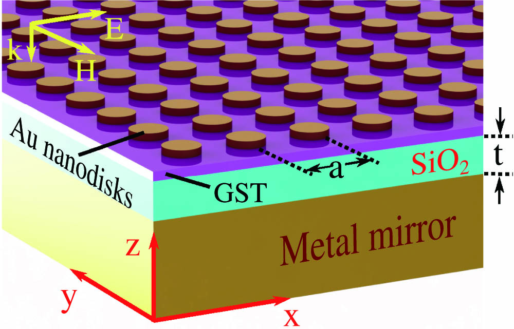
A tunable plasmonic perfect absorber with a tuning range of ~650 nm is realized by introducing a 20 nm thick phase-change material Ge2Sb2Te5 layer into the metal–dielectric–metal configuration. The absorption at the plasmonic resonance is kept above 0.96 across the whole tuning range. In this work we study this extraordinary optical response numerically and reveal the geometric conditions which support this phenomenon. This work shows a promising route to achieve tunable plasmonic devices for multi-band optical modulation, communication, and thermal imaging.
Spectral properties Plasmonics Subwavelength structures, nanostructures Multilayer design Photonics Research
2015, 3(3): 03000054

Author Affiliations
Abstract
1 Department of Physics, Guizhou University, Guiyang 550025, China
2 Laboratory of Optical Physics, Institute of Physics, Chinese Academy of Science, Beijing 100190, China
Surface plasmonic polariton (SPP) waves with complicated wavefronts have important implications in nanophotonic sciences and applications. The surface electromagnetic wave holography method is applied to designed grooves on a metal surface for coupling a plane wave in free space to complicated wavefront SPP waves. The grooves illuminated by the plane wave incident from free space serve as secondary SPP waves sources, that radiate cylindrical SPP waves. New controllable wavefronts originate from these secondary SPP waves interfering with each other, based on the Huygens–Fresnel principle. Several applications of the method are demonstrated, such as converting coupling waves in free space into focusing SPP waves on a metal surface.
050.1970 Diffractive optics 240.6680 Surface plasmons 310.6628 Subwavelength structures,nanostructures Chinese Optics Letters
2015, 13(2): 020501
Author Affiliations
Abstract
A new plasmonic nanolens that can be tuned by varying the circular structure into an elliptical annulus and the aspect ratio from 1 to 0.1 and 1 to 2, respectively, is proposed. Using the rigorous finite-difference and time-domain algorithm, we find that when the aspect ratio ranges from 1 to 0.1, a good linear relationship exists between the aspect ratio and focusing spot size at the full-width at half-maximum in the x- and y-directions, respectively. The corresponding calculated FWHM ranges from 96 × 126 (nm) to 15 \times 52 (nm) (Full Width at Half Maximum).
240.6680 Surface plasmons 310.6628 Subwavelength structures,nanostructures 000.4430 Numerical approximation and analysis 350.5730 Resolution Chinese Optics Letters
2014, 12(1): 012401
Author Affiliations
Abstract
A highly tunable optical nanoantenna element is proposed through gradual transformation from a sphere to a prolate spheroid. This new element induces field enhancement and an increase in resonance frequency. Rather than a purely metallic material, we propose the use of a metal-coated dielectric spheroid as a nanoelement because of its flexibility. We show that a spheroidal element enhances the near-field better than its rod and sphere counterparts. As such, spheroidal elements are good candidates for improving solar-cell performance.
250.5403 Plasmonics 290.2200 Extinction 310.6628 Subwavelength structures,nanostructures 260.2110 Electromagnetic optics Chinese Optics Letters
2013, 11(11): 112503


