1 厦门大学航空航天学院,福建 厦门 361005
2 厦门大学深圳研究院,广东 深圳 518057
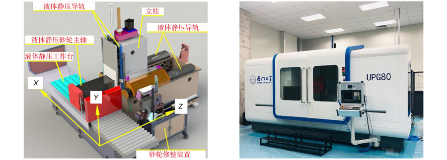
Overview: Driven by the rapid development of national optical projects such as laser nuclear fusion and aerospace telescopes, as well as high-end civilian fields such as advanced instruments and optical lenses, the requirements for full-frequency domain processing errors and surfaces of optical components are becoming more and more stringent. At this stage, the optical components generally need to go through rough grinding, fine grinding, polishing and coating, and other processes, and their surface quality mainly depends on the defect removal ability and error control level of the polishing process. Whether the fine grinding process can obtain better surface shape accuracy and low surface/subsurface damage suppression determines the processing efficiency, and the ultra-precision processing manufacturing equipment is the premise of the realization of ultra-precision machining of the optical components. So far, all countries in the world have invested in the research and development of optical ultra-precision grinding and polishing technology, and have developed more relatively mature high-precision grinding and polishing equipment, which can better meet the processing needs of most of the current optical components. For the core equipment and key technologies required for ultra-precision manufacturing, China has long relied on imports. In order to break through the bottleneck restricting the development of ultra-precision technology in China at this stage, under the traction and drive of the national large-scale engineering project, China has made remarkable progress in optical ultra-precision manufacturing equipment and technology. However, for the optical ultra-precision technology and equipment, there is still a certain gap between China and the international advanced level, and it is necessary to continue to strengthen the research. In addition to the high-end grinding and polishing equipment necessary for the ultra-precision machining of optical components, it is also necessary to strengthen the technical level of a series of key supporting units, such as ultra-precision grinding and polishing processing technology, high-end key functional components, intelligent monitoring technology of processing environment, efficient ultra-precision machining tools, processing and inspection path planning and compensation processing strategies, computer-aided manufacturing and testing software, etc. The research, development, and application of these technologies are related to the development of high-end manufacturing in the civilian fields and national defense fields, and are also the focus of the country. This paper mainly focuses on the ultra-precision machining of large-diameter optical aspherical components. Starting from the grinding and polishing process route, this paper introduces the long-term research progress of the Precision Engineering Laboratory of Xiamen University in the field of large-diameter optical aspherical component processing, and introduces in detail the technical and system achievements such as ultra-precision grinding and polishing equipment, robot-assisted grinding and polishing, equipment intelligent monitoring system, processing technology and control software.
超精密加工 磨抛装备 加工工艺 CAM软件 ultra-precision machining grinding and polishing equipment processing technology CAM software
天津大学精密测试技术及仪器国家重点实验室,微纳制造实验室,天津 300072
介绍了玻璃光学元件精密模压成形技术的原理、玻璃材料、模具制造、模具表面镀膜、结合有限元仿真的模压工艺优化和模压成形设备等核心技术的研究进展,并讨论了当前存在的问题。通过探讨玻璃模压成形技术在自由曲面、微结构、衍射结构表面和晶圆阵列等光学元件中的应用现状,对玻璃元件精密模压成形技术的发展趋势和挑战进行了展望。
光学设计 光学玻璃 非球面透镜 自由曲面透镜 超精密加工 玻璃精密模压 微结构制造
Author Affiliations
Abstract
EPSRC Future Metrology Hub, Centre for Precision Technologies, University of Huddersfield, Huddersfield HD1 3DH, United Kingdom
Freeform optics has become the most prominent element of the optics industry. Advanced freeform optical designs supplementary to ultra-precision manufacturing and metrology techniques have upgraded the lifestyle, thinking, and observing power of existing humans. Imaginations related to space explorations, portability, accessibility have also witnessed sensible in today’s time with freeform optics. Present-day design methods and fabrications techniques applicable in the development of freeform optics and the market requirements are focussed and explained with the help of traditional and non-traditional optical applications. Over the years, significant research is performed in the emerging field of freeform optics, but no standards are established yet in terms of tolerances and definitions. We critically review the optical design methods for freeform optics considering the image forming and non-image forming applications. Numerous subtractive manufacturing technologies including figure correction methods and metrology have been developed to fabricate extreme modern freeform optics to satisfy the demands of various applications such as space, astronomy, earth science, defence, biomedical, material processing, surveillance, and many more. We described a variety of advanced technologies in manufacturing and metrology for novel freeform optics. Next, we also covered the manufacturing-oriented design scheme for advanced optics. We conclude this review with an outlook on the future of freeform optics design, manufacturing and metrology.
freeform optics optical design optical fabrication ultra-precision machining surface metrology International Journal of Extreme Manufacturing
2022, 4(3): 032004
同济大学 物理科学与工程学院 精密光学工程技术研究所,先进微结构材料教育部重点实验室,上海市数字光学前沿科学研究基地,上海市全光谱高性能光学薄膜器件与 应用专业技术服务平台,上海200092
极紫外、X射线为微观物质认识、宏观空间探测提供了高精度的观测手段,但这类观测的实现需要大量高精度光学反射元件的支撑。由于极紫外、X射线在光学表面更易发生散射,其光学反射镜基底的精度需求和制作技术也明显区别于长波元件。近年来,同济大学精密光学工程技术研究所建立了极紫外、X射线反射元件基底的超精密加工与检测平台,研发了超光滑非球面的离子束修形技术,提出了基于泽尼克多项式的随机离轴旋转绝对检测方法,形成了极紫外、X射线光学用反射镜基底的高精度全流程研制技术,并将该技术成功地应用于国内和国际短波光学大科学装置中。本文综述了本课题组在极紫外、X射线用反射镜制作领域中的研究进展。
超精密加工 极紫外 X射线 反射镜基底 非球面元件 绝对检测 ultra-precision machining extreme ultraviolet X-ray reflector substrates aspheric surface absolute measurement 光学 精密工程
2022, 30(21): 2688
1 中国科学院上海光学精密机械研究所精密光学制造与检测中心, 上海 201800
2 中国科学院大学材料科学与光电技术学院, 北京 100049
传统的接触式加工不可避免地会在光学元件上产生亚表层损伤,而大气等离子体抛光(APPP)具有非接触、可定量去除、加工过程不受材料性能影响等优点,在光学加工领域有着巨大的应用潜力。但在实际加工过程中,光学元件加工后的收敛效果并不明显,经验证明去除量随驻留时间的变化呈非线性而导致了加工误差。针对这一问题,首先优化了加工参数;之后研究了加工原理以及加工残余物对后续加工的影响,分析了加工存在非线性效应的原因;提出了一种基于变去除函数的驻留时间算法,并进行了实验验证。结果显示,对尺寸为120 mm×65 mm×10 mm的熔石英光学元件进行变去除函数加工实验,面形峰谷值(PV)的平均收敛率由加工前的21.41%提升至加工后的60.52%,面形均方根值(RMS)的平均收敛率由加工前的24.13%提升至加工后的74.79%,实现了熔石英元件的高精度快速加工,验证了变去除函数加工的有效性。
材料 大气等离子体抛光 去除函数 超精密加工 熔石英 中国激光
2021, 48(24): 2403002
1 南昌航空大学无损检测教育部重点实验室, 江西 南昌 330063
2 中国科学技术大学精密机械与精密仪器系, 安徽 合肥 230026
氟化钙晶体微腔相比玻璃材料微腔,具有吸收系数小、缺陷少、纯度高、对周围环境湿度不敏感的优势,在微波光子学、陀螺仪和非线性光学等领域具有潜在的应用价值。通过超精密加工技术制备了回转椭球体氟化钙毫米晶体微腔。研发了一套精密加工系统来制备这种微腔,所制得的微腔形状为回转椭球体,微腔结构边缘表面粗糙度低至1.97 nm。使用光纤锥波导与氟化钙微腔实现了高效耦合,此耦合系统展现了高达~10 8的超高品质因子Q值和低至约0.03 nm的自由光谱范围。这些结果证明了针对氟化钙微腔的加工手段具有重要意义,将大大促进其应用。氟化钙微腔的特性也证明了它在光学滤波器、腔量子动力学、非线性光学和陀螺仪等应用中的潜力。
光学器件 光学微腔 超精密加工 光学谐振器 回音壁模式
上海交通大学 电子信息与电气工程学院 先进电子材料与器件平台, 上海 200240
文章综述了微透镜阵列制备技术的最新研究进展, 并将这些制备方法分为直接法和间接法进行了对比分析。回顾了微透镜在光场成像应用中的研究进展, 指出目前该领域的研究重点是光场相机设计的新思路及提高分辨率的相应模型算法。
微透镜阵列 光场 光场成像 超精密机械加工 microlens array light field light field imaging ultra-precision machining MEMS MEMS
1 中国科学院上海光学精密机械研究所精密光学制造与检测中心, 上海 201800
2 中国科学院大学材料科学与光电技术学院, 北京 100049
大气等离子体抛光(APPP)是一种非接触式的化学刻蚀加工方法,具有效率高、成本低、精度高等优点,可以作为碳化硅(SiC)加工的一种有效手段。基于APPP气体放电理论和尖端电场畸变效应,分析了电极结构对等离子体放电稳定性和去除函数的影响;从理论上推导了APPP加工SiC的最优电极尖端半径,并进行了实验验证。在最优电极的基础上,系统分析了不同加工参数下APPP刻蚀SiC的去除函数的特性。通过优化电极结构和工艺参数,对直径为50 mm、初始面形误差峰谷(PV)值为475.846 nm、初始面形误差均方根(RMS)为124.771 nm的无压烧结碳化硅(S-SiC)进行加工,加工21 min后,S-SiC工件的PV值降低至103.510 nm,RMS值降低至12.148 nm,RMS收敛率达90.26%。实验结果显示:APPP加工SiC比大多数传统加工方法的效率更高。
表面光学 大气等离子体抛光 碳化硅 去除函数 超精密加工 中国激光
2020, 47(10): 1002002
1 南京航空航天大学自动化学院, 江苏 南京 211100
2 中国地质调查局南京地质调查中心, 江苏 南京 210016
3 江苏三深光谱感知技术研究院有限公司, 江苏 南京 211135
利用矢量衍射理论,对矩形槽型光栅和三角槽型光栅分别进行衍射效率分析,结果表明三角槽型光栅的衍射效率比矩形槽型光栅高出1倍左右。基于五轴超精密单点金刚石车床切削工艺,计算了金刚石刀头移动误差、移动间隔标准偏差范围、光栅刻线位置的加工偏差,并分析了刀头磨损对光栅衍射效率的影响。在此基础上,成功研制了曲率半径为70 mm、刻线密度为60 line/mm、直径为52 mm的凸面闪耀光栅,在1000~2500 nm光谱范围内,其最大相对衍射效率大于80%,平均相对衍射效率大于60%。实际飞行高光谱数据表明,基于该光栅研制的短波红外成像光谱仪满足地质遥感技术要求。
光栅 成像光谱 凸面光栅 衍射效率 超精密加工 短波红外 光学学报
2020, 40(12): 1205002


