

2015, 3(6) Column
Photonics Research 第3卷 第6期

Thermal characteristics are numerically investigated for the hybrid AlGaInAs/InP on silicon microring lasers with different ring radii and widths. Low threshold current and low active region temperature rise are expected for a microring laser with a narrow ring width. Based on the thermal analysis and the 3D simulation for mode characteristics, a hybrid AlGaInAs/InP on silicon microring lasers with an inner n-electrode laterally confined by the p-electrode metallic layer is fabricated using an adhesive bonding technique. A threshold current of 4 mA is achieved for a hybrid microring laser with a radius of 20 μm and a ring width of 3.5 μm at 12°C, and the corresponding threshold current density is as low as 1 kA∕cm2. The influence of the location of silicon waveguide on output performance is studied experimentally for improving the output coupling efficiency. Furthermore, continuous-wave electrically injected lasing up to 55°C is realized for a hybrid microring laser with a radius of 30 μm and a ring width of 3 μm.China under grant 2012AA012202 and NSFC/RGC joint projectunder grant 61431166003. The authors thank Professor Andrew W. Poon and the Nanoelectronics FabricationFacility (NFF) of HKUST for support in the fabrication ofsilicon waveguides.
Semiconductor lasers Semiconductor lasers Photonic integrated circuits Photonic integrated circuits Optical interconnects Optical interconnects 


Impact of multipath effects on theoretical accuracy of TOA-based indoor VLC positioning system Download:1170次
Download:1170次This paper discusses the time-of-arrival (TOA) based indoor visible light communication (VLC) positioning system in a non-line-of-sight environment. The propagation delay is assumed to be gamma distributed. The generalized Cramer–Rao lower bound for multipath propagation is derived as the theoretical accuracy limitation. The performance of the positioning system is affected by the shape parameter and the scale parameter of gamma distribution. The influences on positioning accuracy of multipath effects are analyzed through discussing the physical meaning of the gamma distribution parameters. It is concluded that the lower bound of positioning accuracy is attained when variance of the non-line-of-sight propagation-induced path lengths is zero. The simulation result proves that the theoretical positioning accuracy is in the order of centimeters with the given scenario.
Optical communications Optical communications Free-space optical communication Free-space optical communication 
We theoretically investigate the transport property of graphene surface plasmon polaritons (GSPPs) on curved graphene substrates. The dispersion relationship, propagation length, and field confinement are calculated by an analytical method and compared with those on planar substrates. Based on our theory, the bend of graphene nearly does not affect the property of GSPPs except for an extremely small shift to the lower frequency for the same effective mode index. The field distributions and the eigenfrequencies of GSPPs on planar and cylindrical substrates are calculated by the finite element method, which validates our theoretical analysis. Moreover, three types of graphene-guided optical interconnections of GSPPs, namely, planar to curved graphene film, curved to planar graphene film, and curved to curved graphene film, are proposed and examined in detail. The theoretical results show that the GSPPs propagation on curved graphene substrates and interconnections will not induce any additional losses if the phase-matching condition is satisfied. Additionally, the extreme tiny size of curved graphene for interconnection at a certain spectra range is predicted by our theory and validated by the simulation of 90° turning of GSPPs. The bending effect on the property of GSPPs is systematically analyzed and identified. Our studies would be helpful to instruct design of plasmonic devices involving curved GSPPs, such as nanophotonic circuits, flexible plasmonic, and biocompatible devices.
Surface plasmons Surface plasmons Optical materials Optical materials Optical interconnects Optical interconnects 
Optical trapping and orientation of Escherichia coli cells using two tapered fiber probesDownload:876次
Download:876次We report on the optical trapping and orientation of Escherichia coli (E. coli) cells using two tapered fiber probes. With a laser beam at 980 nm wavelength launched into probe I, an E. coli chain consisting of three cells was formed at the tip of probe I. After launching a beam at 980 nm into probe II, the E. coli at the end of the chain was trapped and oriented via the optical torques yielded by two probes. The orientation of the E. coli was controlled by adjusting the laser power of probe II. Experimental results were interpreted by theoretical analysis and numerical simulations.
Optical tweezers or optical manipulation Optical tweezers or optical manipulation Integrated optics Integrated optics Fiber optics Fiber optics 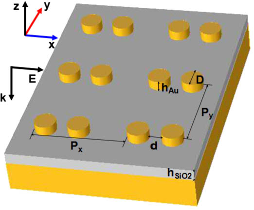
Tunable double-resonance dimer structure for surface-enhanced Raman scattering substrate in near-infrared regionDownload:1007次
Download:1007次Plasmonic resonance with Fano lineshape has attracted a great deal of recent interest. Here we design a new structure with a dimer grating upon a gold film separated by a layer of silica spacer, which has two resonant modes corresponding to the dimer’s localized surface plasmon resonance and the surface plasmon resonance excited by the dimer grating. This structure has three advantages for near-infrared detection in water. First, it provides two resonant modes to enhance the excitation and scattered signals of surface-enhanced Raman scattering. Second, coupling of these two modes results in a Fano resonance, providing a higher electric field enhancement. Finally, the dimer provides more flexible tunability compared to a single disk structure.
Plasmonics Plasmonics Surface-enhanced Raman scattering Surface-enhanced Raman scattering 
A mode transformer based on the quasi-vertical taper is designed to enable high coupling efficiency for interboardlevel optical interconnects involving single-mode polymer waveguides and standard single-mode fibers. A triangular region fabricated above the waveguide is adopted to adiabatically transform the mode from the fiber into the polymer waveguide. The effects of the geometrical parameters of the taper, including width, height, tip width, etc., on the coupling efficiency are numerically investigated. Based on this, a quasi-vertical taper for the polymer rib waveguide system is designed, fabricated, and characterized. Coupling losses of 1.79 _ 0.30 and 2.23 _ 0.31 dB per coupler for the quasi-TM and quasi-TE mode, respectively, are measured across the optical communication C and L bands (1535 to 1610 nm). Low-cost packaging, leading to widespread utilization of polymeric photonic devices, is envisioned for optical interconnect applications.
Buffers Buffers couplers couplers routers routers switches switches and multiplexers and multiplexers Fibers Fibers single-mode single-mode Optical communications Optical communications Polymer waveguides Polymer waveguides Optical design and fabrication Optical design and fabrication Micro-optical devices Micro-optical devices In this paper, we put forward a weak blind quantum signature scheme based on quantum entanglement swapping of Bell states. Different from the existing quantum signature schemes, our scheme can offer two-step verification security services to ensure the validity of the verification. In order to guarantee the unconditional security of the scheme, the quantum key distribution protocol and one-time pad encryption algorithm are employed in our scheme. Besides, the entanglement swapping of Bell states mechanism enhances the security of verification criteria. The proposed scheme has the properties of nonforgeability, nonrepudiation, blindness, and traceability.
Quantum optics Quantum optics Quantum cryptography Quantum cryptography Quantum communications Quantum communications 
Titanium-nitride-based integrated plasmonic absorber/ emitter for solar thermophotovoltaic applicationDownload:1464次
Download:1464次Titanium nitride (TiN) as a refractory plasmonic material is proposed to be used as an angle-insensitive integrated broadband solar absorber and narrowband near-infrared (NIR) emitter for solar thermo-photovoltaic (STPV) application. By constructing TiN-nanopatterns/dielectric/TiN stack metamaterial, approximately 93% light absorption in a wavelength range of 0.3–0.9 μm and near unit narrowband (Δλ∕λ ~ 0.3) emission in NIR (~2 μm) were demonstrated by numerical simulation. Keeping the excellent light absorption in the visible band, the emission wavelength can be easily tuned by patterning the top TiN layer into various subwavelength structures. This dual function attributes to the intrinsic absorption and plasmonic property of TiN. In such an integrated structure, broadband absorption and narrowband emission need to be balanced for an optimized power efficiency conversion. Detailed analysis has demonstrated that the STPV system based on this integrated absorber/emitter can exceed the Shockley–Queisser limit at 1000 K.
Solar energy Solar energy Metamaterials Metamaterials Plasmonics Plasmonics 
We experimentally demonstrated a diode-pumped Kerr-lens mode-locked femtosecond laser with a Yb:CaYAlO4 crystal as the gain medium. Pulse duration as short as 33 fs was obtained directly from the oscillator at a repetition rate of 115 MHz. The central wavelength was at 1059 nm with a spectral bandwidth of 49 nm. These are, to the best of our knowledge, the shortest pulses generated from a Yb:CaYAlO4 oscillator.
Mode-locked lasers Mode-locked lasers Lasers Lasers ytterbium ytterbium Lasers Lasers solid-state solid-state 
The far-field imaging properties of a high index microsphere lens spatially separated from the object are experimentally studied. Our experimental results show that, for a Blu-ray disk whose spacing is 300 nm, the high index microsphere lens also can discern the patterns of the object sample when the distance between the lens and the object is up to 5.4 μm. When the distance is increased from 0 to 5.4 μm, for the microsphere lens with a diameter of 24 μm, the lateral magnification increases from 3.5× to 5.5×, while the field of view decreases from 5.1 to 3.0 μm. By varying the distance between the lens and the object, the optical image can be optimized.We also indicate that the far-field imaging capability of a high index microsphere lens is dependent on the electromagnetic field intensity profile of the photonic nanojet under different positions of the microsphere lens.
Micro-optics Micro-optics Geometric optics Geometric optics Microscopy Microscopy Lenses Lenses 
影响因子:7.6
CN:31-2126/O4
ISSN:2327-9125


公告
动态信息
动态信息 丨 2024-04-25
PR Highlight (Vol. 12, Iss. 2): 封面|超紧凑片上偏振控制器动态信息 丨 2024-04-11
PR Highlight (Vol. 11, Iss. 12): 亮点 | 十亿像素级、高通量的无透镜偏振编码叠层成像技术动态信息 丨 2024-03-29
PR 封面故事 (Vol. 12, Iss. 3): 封面 | 基于时空编码神经网络的像差感知超分辨成像动态信息 丨 2024-03-25
PR 封面故事 (Vol. 12, Iss. 1) 光涡旋与手性器件微纳3D打印动态信息 丨 2024-03-14
PR Highlight (Vol. 12, Iss. 1): 同步双脉冲激光烧蚀中的气泡相互作用效应激光评论微信公众号

点击菜单“联系编辑”即可添加期刊编辑为好友啦