
Author Affiliations
Abstract
1 Zhejiang University, College of Optical Science and Engineering, International Research Center for Advanced Photonics, State Key Laboratory for Modern Optical Instrumentation, Hangzhou, China
2 Zhejiang University, Jiaxing Research Institute, Intelligent Optics & Photonics Research Center, Jiaxing Key Laboratory of Photonic Sensing & Intelligent Imaging, Jiaxing, China
3 Zhejiang University, Ningbo Research Institute, Ningbo, China
Compact passive silicon photonic devices with high performance are always desired for future large-scale photonic integration. Inverse design provides a promising approach to realize new-generation photonic devices, while it is still very challenging to realize complex photonic devices for most inverse designs reported previously due to the limits of computational resources. Here, we present the realization of several representative advanced passive silicon photonic devices with complex optimization, including a six-channel mode (de)multiplexer, a broadband 90 deg hybrid, and a flat-top wavelength demultiplexer. These devices are designed inversely by optimizing a subwavelength grating (SWG) region and the multimode excitation and the multimode interference are manipulated. Particularly, such SWG structures are more fabrication-friendly than those random nanostructures introduced in previous inverse designs. The realized photonic devices have decent performances in a broad bandwidth with a low excess loss of <1 dB, which is much lower than that of previous inverse-designed devices. The present inverse design strategy shows great effectiveness for designing advanced photonic devices with complex requirements (which is beyond the capability of previous inverse designs) by using affordable computational resources.
silicon photonics inverse design subwavelength grating structures mode (de)multiplexers wavelength (de)multiplexers 90 deg hybrids Advanced Photonics Nexus
2023, 2(2): 026005
Author Affiliations
Abstract
1 State Key Laboratory on Integrated Optoelectronics, Institute of Semiconductors, Chinese Academy of Science, Beijing 100083, China
2 College of Materials Science and Opto-Electronic Technology, University of Chinese Academy of Sciences, Beijing 100083, China
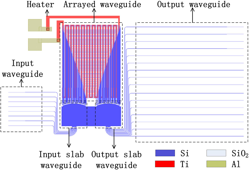
In this Letter, a 16 channel 200 GHz wavelength tunable arrayed waveguide grating (AWG) is designed and fabricated based on the silicon on insulator platform. Considering that the performance of the AWG, such as central wavelength and crosstalk, is sensitive to the dimension variation of waveguides, the error analysis of the AWG with width fluctuations is worked out using the transfer function method. A heater is designed to realize the wavelength tunability of the AWG based on the thermo-optic effect of silicon. The measured results show that the insertion loss of the AWG is about 6 dB, and the crosstalk is 7.5 dB. The wavelength tunability of 1.1 nm is achieved at 276 mW power consumption, and more wavelength shifts will gain at larger power consumption.
060.1810 Buffers, couplers, routers,switches, and multiplexers 060.4230 Multiplexing 230.7390 Waveguides, planar Chinese Optics Letters
2018, 16(1): 010601
Author Affiliations
Abstract
1 State Key Laboratory of Modern Optical Instrumentation, Zhejiang University, Hangzhou 310027, China
2 College of Science, Zhejiang University of Technology, Hangzhou 310028, China
We present compact silicon-arrayed waveguide grating routers (AWGRs) with three different channel spacings of 20, 6.4, and 3.2 nm for optical interconnect systems. The AWGR with the 20 nm channel spacing shows a low loss of 2.5 dB and a low crosstalk of 20 dB and has a footprint of only 0.27 mm×0.19 mm. The AWGR with the channel spacing of 6.4 nm has loss ranging from 3 to 8 dB, and the crosstalk is 18 dB. As for the 3.2 nm channel spacing, the loss is about 4 dB, and the crosstalk is 12 dB.
060.1810 Buffers, couplers, routers,switches, and multiplexers 130.3120 Integrated optics devices 200.4650 Optical interconnects Chinese Optics Letters
2017, 15(3): 030603
中国科学院安徽光学精密机械研究所 中国科学院通用光学定标与表征技术重点实验室, 安徽 合肥 230031
介绍了一种基于现场可编程门阵列(field-programmable gate array, FDGA)的红外光谱信号采集系统实现方案,采用Altera公司的EP2C35系列 的FPGA为控制核心,完成多路模拟开关切换、A/D转换、数据 存取等功能,实现对64路红外光谱信号的采集。同时针对光谱仪输出的微弱直流信号,设计信号调理电路来抑制噪声,最后通过串口通信将数据传给上位机;简介了各 功能模块的实现方案,并进行了实验验证,结果表明该系统的精度和可靠性高,并且最小可检测到0.23 μV的微弱直流信号,实际信噪比达到45 dB。
现场可编程门阵列 红外光谱 信号采集 多路模拟开关 field-programmable gate array infrared spectrum signal acquisition analog multiplexers 大气与环境光学学报
2016, 11(4): 313

Author Affiliations
Abstract
1 Microelectronic Research Center, Department of Electrical and Computer Engineering, The University of Texas atAustin, Austin, Texas 78758, USA
2 Omega Optics, Inc., 8500 Shoal Creek Blvd, Austin, Texas 78757, USA
3 Department of Electrical Engineering and Computer Science, University of Michigan, 1301 Beal Ave, Ann Arbor,Michigan 48109, USA
4 Microelectronic Research Center, Department of Electrical and Computer Engineering, The University of Texas at Austin, Austin, Texas 78758, USA
A mode transformer based on the quasi-vertical taper is designed to enable high coupling efficiency for interboardlevel optical interconnects involving single-mode polymer waveguides and standard single-mode fibers. A triangular region fabricated above the waveguide is adopted to adiabatically transform the mode from the fiber into the polymer waveguide. The effects of the geometrical parameters of the taper, including width, height, tip width, etc., on the coupling efficiency are numerically investigated. Based on this, a quasi-vertical taper for the polymer rib waveguide system is designed, fabricated, and characterized. Coupling losses of 1.79 _ 0.30 and 2.23 _ 0.31 dB per coupler for the quasi-TM and quasi-TE mode, respectively, are measured across the optical communication C and L bands (1535 to 1610 nm). Low-cost packaging, leading to widespread utilization of polymeric photonic devices, is envisioned for optical interconnect applications.
Buffers Buffers couplers couplers routers routers switches switches and multiplexers and multiplexers Fibers Fibers single-mode single-mode Optical communications Optical communications Polymer waveguides Polymer waveguides Optical design and fabrication Optical design and fabrication Micro-optical devices Micro-optical devices Photonics Research
2015, 3(6): 06000317
Author Affiliations
Abstract
Electronic Engineering of National Kaohsiung University of Applied Sciences, Kaohsiung 807, China
In this work, we propose a new design of all-optical triplexer based on of metal–insulator–metal (MIM) plasmonic waveguide structures and ring resonators. By adjusting the radii of ring resonators and the gap distance, certain wavelengths can be filtered out and the crosstalk of each channel can also be reduced. The numerical results show that the proposed MIM plasmonic waveguide structure can really function as an -optical triplexer with respect to the three wavelengths, that is, 1310, 1490, and 1550 nm, respectively. It can be widely used as the fiber access network element for multiplexer–demultiplexer wavelength selective in -fiber-to-the-home communication systems with transmission efficiency higher than 90%. It can also be a potential key component in the applications of the biosensing systems.
060.1810 Buffers, couplers, routers,switches, and multiplexers 130.7408 Wavelength filtering devices 130.3120 Integrated optics devices 230.5750 Resonators Chinese Optics Letters
2014, 12(11): 110607
Author Affiliations
Abstract
A hybrid optical switch (HOS) with physical layer of wavelength division multiplexing and optical code division multiplexing (WDM/OCDM) scheme is proposed. An additional feature to the HOS than optical cross connect (OXC) is that the controller can process requests for both circuit establishment and burst scheduling. In our study, the measurement criteria of HOS are the blocking probability, probability of error, and probability of outage. To simplify the analysis, no distinction is made between a circuit in progress and a burst in progress. Moreover, a minimum fit (MinF) resource allocation strategy is applied in order to increase the bandwidth efficiency and control the multiplexing interference of the OCDM. A 2D Markov model for the HOS is presented using the MinF strategy. Numerical results reveal that the code parameters and the resource allocation strategy greatly affect the performance. Certain periority can be achieved by assigning shorter codes to high periority users and longer codes to low periority users. Also, the probability of error and outage are reduced by appling the MinF strategy.
060.0060 Fiber optics and optical communications 060.1155 All-optical networks 060.1660 Coherent communications 060.1810 Buffers, couplers, routers,switches, and multiplexers 060.2310 Fiber optics Chinese Optics Letters
2014, 12(5): 050602
Author Affiliations
Abstract
A novel fiber Bragg grating (FBG) sensing system based on code division multiple access (CDMA) technology is proposed. CDMA is used to separate each reflected sensor. Simulation of experimental results indicates the CDMA technology combines with optical fiber grating sensing system together successfully. Furthermore, the system using semiconductor optical amplifier (SOA) is experimented. The experimental results show that theory and simulation are correct.
060.3735 Fiber Bragg gratings 060.1810 Buffers, couplers, routers,switches, and multiplexers 060.4230 Multiplexing Chinese Optics Letters
2013, 11(s2): S20602
Author Affiliations
Abstract
1 Department of Electronic Engineering, Xiamen University, Xiamen 361005, China
2 Department of Physics, Xiamen University, Xiamen 361005, China
A novel scheme is proposed, in which the aberrations in the off-axis holographic lenses used as demultiplexers are reduced to a low enough level for relatively small channel spacing. The scheme includes optimizing the recording and reconstruction geometries and collimating the reconstruction wave with a gradient-index lens. A demultiplexer operated in the 1 550-nm band with 5-nm channel spacing and ?\infty-dB crosstalk is obtained using the scheme. The channel spacing can be decreased to 2 nm by etching the cladding of the output fibers to a smaller size.
解复用器 全息透镜 离轴 单色像差 060.1810 Buffers, couplers, routers,switches, and multiplexers 090.2890 Holographic optical elements 090.1000 Aberration compensation Chinese Optics Letters
2011, 9(9): 090603


