1 Institute of Nanophotonics, Jinan University, Guangzhou 511443, China
2 e-mail: liyuchao@jnu.edu.cn
3 e-mail: zhyao5@jnu.edu.cn
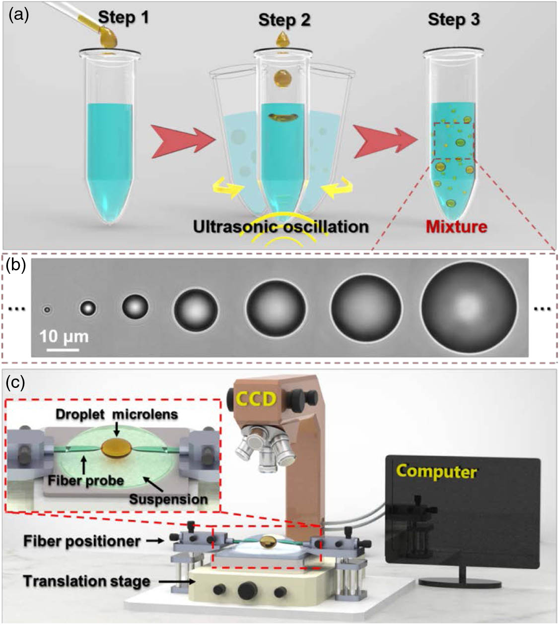
We developed adjustable and movable droplet microlenses consisting of a liquid with a high refractive index. The microlenses were prepared via ultrasonic shaking in deionized water, and the diameter of the microlenses ranged from 1 to 50 μm. By stretching the microlenses, the focal length can be adjusted from 13 to 25 μm. With the assistance of an optical tweezer, controllable assembly and movement of microlens arrays were also realized. The results showed that an imaging system combined with droplet microlenses could image 80 nm beads under white light illumination. Using the droplet microlenses, fluorescence emission at 550 nm from CdSe@ZnS quantum dots was efficiently excited and collected. Moreover, Raman scattering signals from a silicon wafer were enhanced by times. The presented droplet microlenses may offer new opportunities for flexible liquid devices in subwavelength imaging and detection.
1 Beijing National Research Center for Information Science and Technology (BNRist), Beijing Innovation Center for Future Chips, Electronic Engineering Department, Tsinghua University, Beijing 100084, China
2 Institute of Fundamental and Frontier Sciences, University of Electronic Science and Technology of China, Chengdu 610054, China
3 Frontier Science Center for Quantum Information, Beijing 100084, China
4 Beijing Academy of Quantum Information Sciences, Beijing 100193, China
We propose a hybrid silicon waveguide scheme to avoid the impact of noise photons induced by pump lights in application scenarios of quantum photonic circuits with quantum light sources. The scheme is composed of strip waveguide and shallow-ridge waveguide structures. It utilizes the difference of biphoton spectra generated by spontaneous four-wave mixing (SFWM) in these two waveguides. By proper pumping setting and signal/idler wavelength selection, the generation of desired photon pairs is confined in the strip waveguide. The impact of noise photons generated by SFWM in the shallow-ridge waveguide can be avoided. Hence, the shallow-ridge waveguide could be used to realize various linear operation devices for pump light and quantum state manipulations. The feasibility of this scheme is verified by theoretical analysis and a primary experiment. Two applications are proposed and analyzed, showing its great potential in silicon-based quantum photonic circuits.
1 Guangzhou Key Laboratory for Special Fiber Photonic Devices and Applications & Guangdong Provincial Key Laboratory of Nanophotonic Functional Materials and Devices, South China Normal University, Guangzhou 510006, China
2 e-mail: xuwch@scnu.edu.cn
3 e-mail: zcluo@scnu.edu.cn
We report the “periodic” soliton explosions induced by intracavity soliton collisions in a dual-wavelength mode-locked Yb-doped fiber laser. Owing to the different group velocities of the two wavelengths, the mode-locked solitons centered at different wavelengths would periodically collide with each other. By using the dispersive Fourier transformation technique, it was found that each collision would induce soliton explosions, but none of them would be identical. Therefore, this phenomenon was termed as “periodic” soliton explosions. In addition, the dissipative rogue waves were detected in the dual-wavelength mode-locked state. The experimental results would be fruitful to the communities interested in soliton dynamics and dual-comb lasers.
1 School of Optical Science and Engineering, University of New Mexico, Albuquerque, New Mexico 87106, USA
2 Department of Physics and Astronomy, University of New Mexico, Albuquerque, New Mexico 87131, USA
3 Center for High Technology Materials, University of New Mexico, Albuquerque, New Mexico 87106, USA
4 NASA Marshall Space Flight Center, Space Systems Department, Huntsville, Alabama 35812, USA
An equivalence is made between the exceptional points proposed by the field of non-Hermitian quantum mechanics and the dead band observed in laser gyroscopes. The sensitivity enhancement near this exceptional point is plagued by increased uncertainty due to broadening of the beat-note bandwidth. Also, near the dead band the gyroscope response is caused by Rabi intensity oscillations and not solely by a phase modulation. Finally, a distinction is made between conservative and non-conservative coupling.
1 Institute of Microscale Optoelectronics, Shenzhen University, Shenzhen 518052, China
2 School of Physics, State Key Laboratory of Crystal Materials, Shandong University, Jinan 250100, China
3 Departamento Física Aplicada, Facultad Ciencias, Universidad de Salamanca, Salamanca 37008, Spain
We fabricated a three-dimensional microstructured optical waveguide (MOW) in a single-crystal using the femtosecond-laser writing and phosphoric acid etching techniques, and observed excellent midinfrared waveguiding performance with low loss of . Tracks with a periodic arrangement were written inside the yttrium aluminum garnet (YAG) crystal via femtosecond laser inscription, and then etched by the phosphoric acid () to form the hollow structures. The evolution of the microstructure of tracks was investigated in detail. The function of the MOW was analyzed by different numerical methods, indicating the proposed MOW can effectively operate in quasi-single-mode pattern in the midinfrared wavelength range, which agrees well with our experiment results.
1 College of Computer, National University of Defense Technology, Changsha 410073, China
2 College of Advanced Interdisciplinary Studies, National University of Defense Technology, Changsha 410073, China
3 National Innovation Institute of Defense Technology, Academy of Military Sciences PLA China, Beijing 100071, China
Metamaterials play an important role in the modulation of amplitude and group delay in the terahertz (THz) regime on account of their optical properties, which are rare in natural materials. Here an ultrafast anisotropic switch of the plasmon-induced transparency (PIT) effect is experimentally and numerically demonstrated by metamaterial devices composed of two pairs of planar split-ring resonators and a pair of closed-ring resonators. By integration with a germanium (Ge) film, a recovery time of 3 ps and a decay constant of 785 fs are realized in the metadevice. Stimulated by the exterior optical pump, the PIT windows at different frequencies are switched off with an excellent property of slow light for vertical and horizontal THz polarizations, realizing an astonishing modulation depth as high as 99.06%. This work provides a new platform for ultrafast anisotropic metadevices tunable for amplitude and group delay.
1 Department of Electrical and Computer Engineering, National University of Singapore, Singapore 117576, Singapore
2 Institute of Laser Engineering, Beijing University of Technology, Beijing 100124, China
3 e-mail: ncltji@bjut.edu.cn
This paper reports the physical phenomenon of the temporal overlapping double femtosecond laser-induced ablation enhancement at different time delays. Detailed thermodynamic modeling demonstrates the ablation enhancement is highly dependent on the first pulse’s laser fluence. In the case of the first pulse laser fluence being higher than material’s ablation threshold, the ablation enhancement is attributed to optical absorption modification by the first pulse ablation. While the first pulse’s laser fluence is lower than the material’s ablation threshold, the first pulse-induced melting leads to much higher absorption of the second pulse. However, for the case of the first pulse’s laser fluence even lower than melting threshold, the ablation enhancement decreases obviously with time delay. The results of the temporal overlapping double femtosecond laser ablation of poly(-caprolactone) are in good agreement with the theoretical predictions.
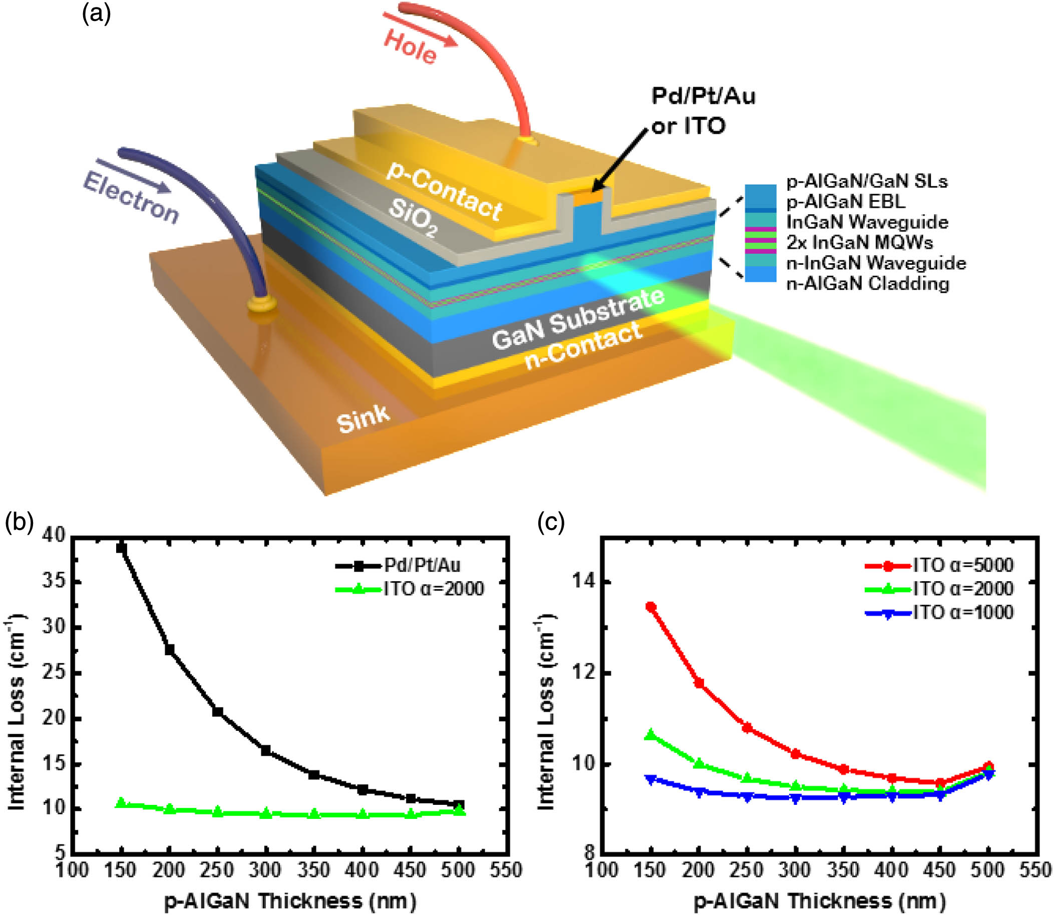
1 Key Laboratory of Nanodevices and Applications, Suzhou Institute of Nano-Tech and Nano-Bionics, Chinese Academy of Sciences (CAS), Suzhou 215123, China
2 School of Nano-Tech and Nano-Bionics, University of Science and Technology of China, Hefei 230026, China
Green laser diodes (LDs) still perform worst among the visible and near-infrared spectrum range, which is called the “green gap.” Poor performance of green LDs is mainly related to the p-type AlGaN cladding layer, which on one hand imposes large thermal budget on InGaN quantum wells (QWs) during epitaxial growth, and on the other hand has poor electrical property especially when low growth temperature has to be used. We demonstrate in this work that a hybrid LD structure with an indium tin oxide (ITO) p-cladding layer can achieve threshold current density as low as , which is only one third of that of the conventional LD structure. The improvement is attributed to two benefits that are enabled by the ITO cladding layer. One is the reduced thermal budget imposed on QWs by reducing p-AlGaN layer thickness, and the other is the increasing hole concentration since a low Al content p-AlGaN cladding layer can be used in hybrid LD structures. Moreover, the slope efficiency is increased by 25% and the operation voltage is reduced by 0.6 V for hybrid green LDs. As a result, a 400 mW high-power green LD has been obtained. These results indicate that a hybrid LD structure can pave the way toward high-performance green LDs.
1 State Key Laboratory of Optoelectronic Materials and Technologies, School of Materials, Sun Yat-sen University, Guangzhou 510275, China
2 Key Laboratory of Materials Physics, Institute of Solid State Physics, Chinese Academy of Sciences, Hefei 230031, China
This erratum corrects the errors that appeared in Photon. Res.6, 709 (2018)PRHEIZ2327-912510.1364/PRJ.6.000709 associated with the polarization description of the experimental optical path, as well as the image errors.
Wuhan National Laboratory for Optoelectronics (WNLO), Huazhong University of Science and Technology, Wuhan 430074, China
The radical suppression of the photodarkening effect and laser performance deterioration via loading were demonstrated in high-power Yb-doped fiber (YDF) amplifiers. The photodarkening loss at equilibrium was 114.4 dB/m at 702 nm in the pristine fiber, while it vanished in the -loaded fiber. To obtain a deeper understanding of the impact of photodarkening on laser properties, the evolution of the mode instability threshold and output power in fiber amplifiers was investigated. After pumping for 300 min, the mode instability threshold of the pristine fiber dropped from 770 to 612 W, and the periodic fluctuation of the output power became intense, finally reaching 100 W. To address the detrimental effects originating from photodarkening, loading was applied in contrast experiments. The output power remained stable, and no sign of mode instability was observed in the -loaded fiber. Moreover, the transmittance at 638 nm confirmed the absence of the photodarkening effect. The results pave the way for the further development of high-power fiber lasers.
1 Center for Quantum Information, Korea Institute of Science and Technology, Seoul 02792, South Korea
2 Division of Nano and Information Technology, Korea Institute of Science and Technology School, Korea University of Science and Technology, Seoul 02792, South Korea
Quantum key distribution (QKD) networks constitute promising solutions for secure communication. Beyond conventional point-to-point QKD, we developed 1 × N QKD network systems with a sub-nanosecond resolution optical path length compensation scheme. With a practical plug-and-play QKD architecture and compact timing control modules based on a field-programmable gate array, we achieved long-term stable operation of a QKD network system. Using this architecture, 64 users can simultaneously share secret keys with one server, without using complex software algorithms and expensive hardware. We demonstrated the workings of a QKD network system using the fiber network of a metropolitan area.
1 Key Laboratory of Optoelectronic Materials and Technologies, School of Electrical and Information Technology, Sun Yat-sen University, Guangzhou 510275, China
2 Southern Marine Science and Engineering Guangdong Laboratory (Zhuhai), Zhuhai 519000, China
3 Department of Electronic Engineering, College of Information Science and Technology, Jinan University, Guangzhou 510632, China
4 e-mail: zhangbin5@mail.sysu.edu.cn
5 e-mail: lzhh88@mail.sysu.edu.cn
Fast and sensitive air-coupled ultrasound detection is essential for many applications such as radar, ultrasound imaging, and defect detection. Here we present a novel approach based on a digital optical frequency comb (DOFC) technique combined with high- optical microbubble resonators (MBRs). DOFC enables precise spectroscopy on resonators that can trace the ultrasound pressure with its resonant frequency shift with femtometer resolution and sub-microsecond response time. The noise equivalent pressure of air-coupled ultrasound as low as is achieved by combining a high- () MBR with the DOFC method. Moreover, it can observe multi-resonance peaks from multiple MBRs to directly monitor the precise spatial location of the ultrasonic source. This approach has a potential to be applied in 3D air-coupled photoacoustic and ultrasonic imaging.
1 MOE Key Laboratory of Weak-Light Nonlinear Photonics, TEDA Institute of Applied Physics and School of Physics, Nankai University, Tianjin 300457, China
2 Collaborative Innovation Center of Extreme Optics, Shanxi University, Taiyuan 030006, China
3 e-mail: zhanggq@nankai.edu.cn
4 e-mail: jjxu@nankai.edu.cn
A fabrication process allowing for the production of periodically poled lithium niobate (PPLN) photonic devices with any domain pattern and unit size down to 200 nm is developed by combining semiconductor fabrication techniques and piezo-force-microscopy tips polarization. Based on this fabrication process, PPLN microdisk resonators with quality factors of were fabricated from a Z-cut lithium niobate film. Second-harmonic generation (SHG) utilizing in the whole cavity was demonstrated in a PPLN microdisk with a 2 μm-spatial-period radial domain pattern. The SHG conversion efficiency was measured to be . This work paves the way to fabricate complex PPLN photonic devices and to obtain efficient nonlinear optical effects that have wide applications in both classical and quantum optics.
1 Institute of Photonics, Department of Physics, Technology and Innovation Centre, University of Strathclyde, Glasgow G1 1RD, UK
2 Diamond Science and Technology, Centre for Doctoral Training, University of Warwick, Coventry CV4 7AL, UK
3 School of Engineering, University of Glasgow, Glasgow G12 8LT, UK
High-quality integrated diamond photonic devices have previously been demonstrated in applications from non-linear photonics to on-chip quantum optics. However, the small sample sizes of single crystal material available, and the difficulty in tuning its optical properties, are barriers to the scaling of these technologies. Both of these issues can be addressed by integrating micrometer-scale diamond devices onto host photonic integrated circuits using a highly accurate micro-assembly method. In this work a diamond micro-disk resonator is integrated with a standard single-mode silicon-on-insulator waveguide, exhibiting an average loaded -factor of across a range of spatial modes, with a maximum loaded -factor of . The micrometer-scale device size and high thermal impedance of the silica interface layer allow for significant thermal loading and continuous resonant wavelength tuning across a 450 pm range using a milliwatt-level optical pump. This diamond-on-demand integration technique paves the way for tunable devices coupled across large-scale photonic circuits.
School of Instrumentation and Optoelectronic Engineering, Beihang University, Beijing 100191, China
First-photon imaging is a photon-efficient, computational imaging technique that reconstructs an image by recording only the first-photon arrival event at each spatial location and then optimizing the recorded photon information. The optimization algorithm plays a vital role in image formation. A natural scene containing spatial correlation can be reconstructed by maximum likelihood of all spatial locations constrained with a sparsity regularization penalty, and different penalties lead to different reconstructions. The -norm penalty of wavelet transform reconstructs major features but blurs edges and high-frequency details of the image. The total variational penalty preserves edges better; however, it induces a “staircase effect,” which degrades image quality. In this work, we proposed a hybrid penalty to reconstruct better edge features while suppressing the staircase effect by combining wavelet -norm and total variation into one penalty function. Results of numerical simulations indicate that the proposed hybrid penalty reconstructed better images, which have an averaged root mean square error of 12.83%, 5.68%, and 10.56% smaller than those of the images reconstructed by using only wavelet -norm penalty, total variation penalty, or recursive dyadic partitions method, respectively. Experimental results are in good agreement with the numerical ones, demonstrating the feasibility of the proposed hybrid penalty. Having been verified in a first-photon imaging system, the proposed hybrid penalty can be applied to other noise-removal optimization problems.
1 Department of Electrical Engineering and Computer Science, University of Michigan, Ann Arbor, Michigan 48109, USA
2 Department of Materials Science and Engineering, University of Michigan, Ann Arbor, Michigan 48109, USA
AlGaN is the material of choice for high-efficiency deep UV light sources, which is the only alternative technology to replace mercury lamps for water purification and disinfection. At present, however, AlGaN-based mid- and deep UV LEDs exhibit very low efficiency. Here, we report a detailed investigation of the epitaxy and characterization of LEDs utilizing an AlGaN/GaN/AlGaN tunnel junction structure, operating at , which have the potential to break the efficiency bottleneck of deep UV photonics. A thin GaN layer was incorporated between and -AlGaN to reduce the tunneling barrier. By optimizing the thickness of the GaN layer and thickness of the top -AlGaN contact layer, we demonstrate AlGaN deep UV LEDs with a maximum external quantum efficiency of 11% and wall-plug efficiency of 7.6% for direct on-wafer measurement. It is also observed that the devices exhibit severe efficiency droop under low current densities, which is explained by the low hole mobility, due to the hole hopping conduction in the Mg impurity band and the resulting electron overflow.
Department of Physics, Pusan National University, Geumjeong-Gu, Busan 46241, South Korea
An understanding of the phenomenon of light interference forms the kernel underlying the discovery of the nature of light from the viewpoints of both classical physics and quantum physics. Here we report on two-photon interference with temporally separated continuous-wave coherent photons by using a temporal post-selection method with an arbitrary time delay. Although the temporal separation of a day between the photons is considerably longer than the coherence time of the light source, we observe the Hong–Ou–Mandel (HOM) interference of the pairwise two-photon state. Furthermore, we experimentally demonstrate the HOM interference observed in one of the interferometer-output modes by using only one single-photon detector for a large temporal separation.
1 School of Physics and Optoelectronic Technology, South China University of Technology, Guangzhou 510640, China
2 School of Physics, Peking University, Beijing 100871, China
Vacuum Rabi splitting, which stems from a single photon interaction with a quantum emitter (a single atom, molecule, or quantum dot), is a fundamental quantum phenomenon. Many reports have claimed that using J aggregate coupling to highly localized plasmon can produce giant Rabi splitting (in scattering spectra) that is proportional to , where is the number of excitons in J aggregates, and this splitting originates purely from quantum interaction between excitons and plasmons. In this work, we show that the scattering spectra are very sensitive to the surrounding matter, and the giant spectral splitting stems both from the quantum interaction of a single molecule with plasmons (Rabi splitting) and from the classical optical interaction of multiple molecules with plasmons. We develop a Lorentzian model to describe molecules and plasmon and find that the collective optical interaction is dominant in generating the giant splitting (in scattering spectra), which is also proportional to , upon the quantum interaction of single-molecule Rabi splitting. Simply speaking, the observed giant spectral splitting is not a pure quantum Rabi splitting effect, but rather a mixture contribution from the large spectral modulation by the collective optical interaction of all molecules with plasmons and the modest quantum Rabi splitting of a single molecule strongly coupled with plasmons.
1 Centre for Nanoscience and Nanotechnology (C2N), CNRS, Université Paris-Sud, Université Paris-Saclay, UMR 9001, 91405 Orsay Cedex, France
2 Technologie R&D, STMicroelectronics, SAS, 850 rue Jean Monnet, 38920 Crolles, France
3 III-V lab, a joint venture from Nokia Bell Labs, Thales and CEA, 1 Avenue Augustin Fresnel, 91767 Palaiseau Cedex, France
We report supercontinuum generation in nitrogen-rich (N-rich) silicon nitride waveguides fabricated through back-end complementary-metal-oxide-semiconductor (CMOS)-compatible processes on a 300 mm platform. By pumping in the anomalous dispersion regime at a wavelength of 1200 nm, two-octave spanning spectra covering the visible and near-infrared ranges, including the O band, were obtained. Numerical calculations showed that the nonlinear index of N-rich silicon nitride is within the same order of magnitude as that of stoichiometric silicon nitride, despite the lower silicon content. N-rich silicon nitride then appears to be a promising candidate for nonlinear devices compatible with back-end CMOS processes.
1 Instituto de Óptica Daza de Valdés, Consejo Superior de Investigaciones Científicas (CSIC), Madrid 28006, Spain
2 Departamento de Ingeniería de Comunicaciones, ETSI Telecomunicación, Universidad de Málaga, Málaga 29071, Spain
3 National Research Council Canada, Ottawa K1A 0R6, Canada
4 Bionand Center for Nanomedicine and Biotechnology, Parque Tecnológico de Andalucía, Málaga 29590, Spain
Optical phase shifters are extensively used in integrated optics not only for telecom and datacom applications but also for sensors and quantum computing. While various active solutions have been demonstrated, progress in passive phase shifters is still lacking. Here we present a new type of ultra-broadband 90° phase shifter, which exploits the anisotropy and dispersion engineering in subwavelength metamaterial waveguides. Our Floquet–Bloch calculations predict a phase-shift error below over an unprecedented operation range from 1.35 to 1.75 μm, i.e., 400 nm bandwidth covering the E, S, C, L, and U telecommunication bands. The flat spectral response of our phase shifter is maintained even in the presence of fabrication errors up to , showing greater robustness than conventional structures. Our device was experimentally demonstrated using standard 220 nm thick SOI wafers, showing a fourfold reduction in the phase variation compared to conventional phase shifters within the 145 nm wavelength range of our measurement setup. The proposed subwavelength engineered phase shifter paves the way for novel photonic integrated circuits with an ultra-broadband performance.
1 Key Laboratory of Optoelectronics Information Technology (Tianjin University), Ministry of Education, School of Precision Instruments and Optoelectronics Engineering, Tianjin University, Tianjin 300072, China
2 Department of Applied Physics and Materials, Research Centre, The Hong Kong Polytechnic University, Hong Kong, China
3 National Institute for Advanced Materials, Tianjin Key Laboratory of Metal and Molecule Based Material Chemistry, Key Laboratory of Functional Polymer Materials, Collaborative Innovation Center of Chemical Science and Engineering (Tianjin), School of Materials Science and Engineering, Nankai University, Tianjin 300071, China
4 e-mail: shengquan@tju.edu.cn
5 e-mail: apafyan@polyu.edu.hk
6 e-mail: jqyao@tju.edu.cn
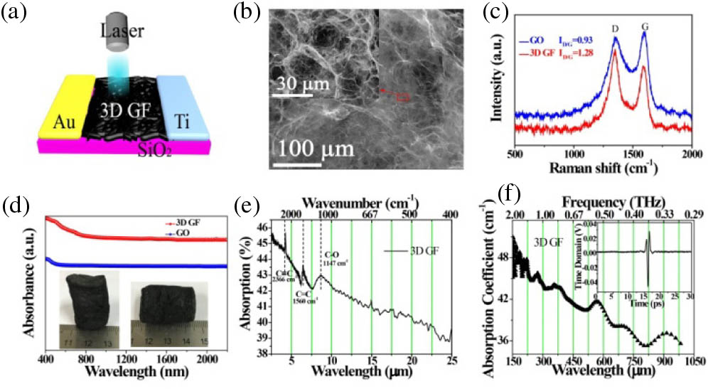
Highly sensitive broadband photodetection is of critical importance for many applications. However, it is a great challenge to realize broadband photodetection by using a single device. Here we report photodetectors (PDs) based on three-dimensional (3D) graphene foam (GF) photodiodes with asymmetric electrodes, which show an ultra-broadband photoresponse from ultraviolet to microwave for wavelengths ranging from to . Moreover, the devices exhibit a high photoresponsivity of , short response time of 43 ms, and 3 dB bandwidth of 80 Hz. The high performance of the devices can be attributed to the photothermoelectric (PTE, also known as the Seebeck) effect in 3D GF photodiodes. The excellent optical, thermal, and electrical properties of 3D GFs offer a superior basis for the fabrication of PTE-based PDs. This work paves the way to realize ultra-broadband and high-sensitivity PDs operated at room temperature.
Department of Electrical and Computer Engineering, Center for Optical Materials Science and Engineering Technologies, Clemson University, Clemson, South Carolina 29634, USA
Chip-scale, tunable narrow-linewidth hybrid integrated diode lasers based on quantum-dot RSOAs at 1.3 μm are demonstrated through butt-coupling to a silicon nitride photonic integrated circuit. The hybrid laser linewidth is around 85 kHz, and the tuning range is around 47 nm. Then, a fully integrated beam steerer is demonstrated by combining the tunable diode laser with a waveguide surface grating. Our system can provide beam steering of 4.1° in one direction by tuning the wavelength of the hybrid laser. Besides, a wavelength-tunable triple-band hybrid laser system working at , , and bands is demonstrated for wide-angle beam steering in a single chip.
1 School of Electrical and Computer Engineering, Ben-Gurion University of the Negev, Beer-Sheva 84105, Israel
2 Electrical and Electronics Engineering Department, Shamoon College of Engineering, Beer-Sheva 84100, Israel
3 School of Electrical Engineering, The Jerusalem College of Technology, Jerusalem 91160, Israel
4 Ilse Katz Institute for Nanoscale Science & Technology, Ben-Gurion University of the Negev, Beer-Sheva 84105, Israel
We propose a novel concept of designing silicon photonics metamaterials for perfect near-infrared light absorption. The study’s emphasis is an in-depth investigation of various physical mechanisms behind the ultra-narrowband record peak absorptance of the designed structures, comprising an ultrathin silicon absorber. The electromagnetic power transport, described by the Poynting vector, is innovatively explored, which shows combined vortex and crossed-junction two-dimensional waveguide-like flows as outcomes of optical field singularities. These flows, though peculiar for each of the designed structures, turn out to be key factors of the perfect resonant optical absorption. The electromagnetic fields show tight two-dimensional confinement: a sharp vertical confinement of the resonant-cavity type combined with a lateral metasurface supported confinement. The silicon-absorbing layer and its oxide environment are confined between two subwavelength metasurfaces such that the entire design is well compatible with silicon-on-insulator microelectronics. The design concept and its outcomes meet the extensive challenges of ultrathin absorbers for minimum noise and an ultra-narrowband absorptance spectrum, while maintaining an overall very thin structure for planar integration. With these materials and such objectives, the proposed designs seem essential, as standard approaches fail, mainly due to a very low silicon absorption coefficient over the near-infrared range. Tolerance tests for fabrication errors show fair tolerability while maintaining a high absorptance peak, along with a controllable deviation off the central-design wavelength. Various applications are suggested and analyzed, which include but are not limited to: efficient photodetectors for focal plane array and on-chip integrated silicon photonics, high-precision spectroscopic chemical and angular-position sensing, and wavelength-division multiplexing.
1 Key Laboratory of Photoelectronic Imaging Technology and System, School of Optics and Photonics, Beijing Institute of Technology, Beijing 100081, China
2 School of Computer Science and Information Security, Guilin University of Electronic Technology, Guilin 541004, China
3 Department of Electrical and Computer Engineering, University of Delaware, Newark, Delaware 19716, USA
4 e-mail: ciom_xtf1@bit.edu.cn
5 e-mail: maxu@bit.edu.cn
Coded apertures with random patterns are extensively used in compressive spectral imagers to sample the incident scene in the image plane. Random samplings, however, are inadequate to capture the structural characteristics of the underlying signal due to the sparsity and structure nature of sensing matrices in spectral imagers. This paper proposes a new approach for super-resolution compressive spectral imaging via adaptive coding. In this method, coded apertures are optimally designed based on a two-tone adaptive compressive sensing (CS) framework to improve the reconstruction resolution and accuracy of the hyperspectral imager. A liquid crystal tunable filter (LCTF) is used to scan the incident scene in the spectral domain to successively select different spectral channels. The output of the LCTF is modulated by the adaptive coded aperture patterns and then projected onto a low-resolution detector array. The coded aperture patterns are implemented by a digital micromirror device (DMD) with higher resolution than that of the detector. Due to the strong correlation across the spectra, the recovered images from previous spectral channels can be used as a priori information to design the adaptive coded apertures for sensing subsequent spectral channels. In particular, the coded apertures are constructed from the a priori spectral images via a two-tone hard thresholding operation that respectively extracts the structural characteristics of bright and dark regions in the underlying scenes. Super-resolution image reconstruction within a spectral channel can be recovered from a few snapshots of low-resolution measurements. Since no additional side information of the spectral scene is needed, the proposed method does not increase the system complexity. Based on the mutual-coherence criterion, the proposed adaptive CS framework is proved theoretically to promote the sensing efficiency of the spectral images. Simulations and experiments are provided to demonstrate and assess the proposed adaptive coding method. Finally, the underlying concepts are extended to a multi-channel method to compress the hyperspectral data cube in the spatial and spectral domains simultaneously.
1 State Key Laboratory of Optoelectronic Materials and Technologies, School of Physics and Engineering, Sun Yat-sen University, Guangzhou 510275, China
2 Institute of Optoelectronics, Shenzhen University, Shenzhen 518060, China
3 Institute of Solid State Physics, Chinese Academy of Sciences, Hefei 230031, China
4 e-mail: rszheng@szu.edu.cn
This erratum corrects errors that appeared in Photon. Res.3, 38 (2015)PRHEIZ2327-912510.1364/PRJ.3.000038 related to the polarization of the experimental optical path and a few typos.
1 School of Physics and Optoelectronics, South China University of Technology, Guangzhou 510640, China
2 State Key Laboratory of Luminescent Materials and Devices and Institute of Optical Communication Materials, South China University of Technology, Guangzhou 510640, China
3 Guangdong Engineering Technology Research and Development Center of High-performance Fiber Laser Techniques and Equipment, Zhuhai 519031, China
4 Hengqin Firay Sci-Tech Company Ltd., Zhuhai 519031, China
5 Guangdong Engineering Technology Research and Development Center of Special Optical Fiber Materials and Devices, Guangzhou 510640, China
6 Guangdong Provincial Key Laboratory of Fiber Laser Materials and Applied Techniques, South China University of Technology, Guangzhou 510640, China
7 e-mail: pengfeima_scut@163.com
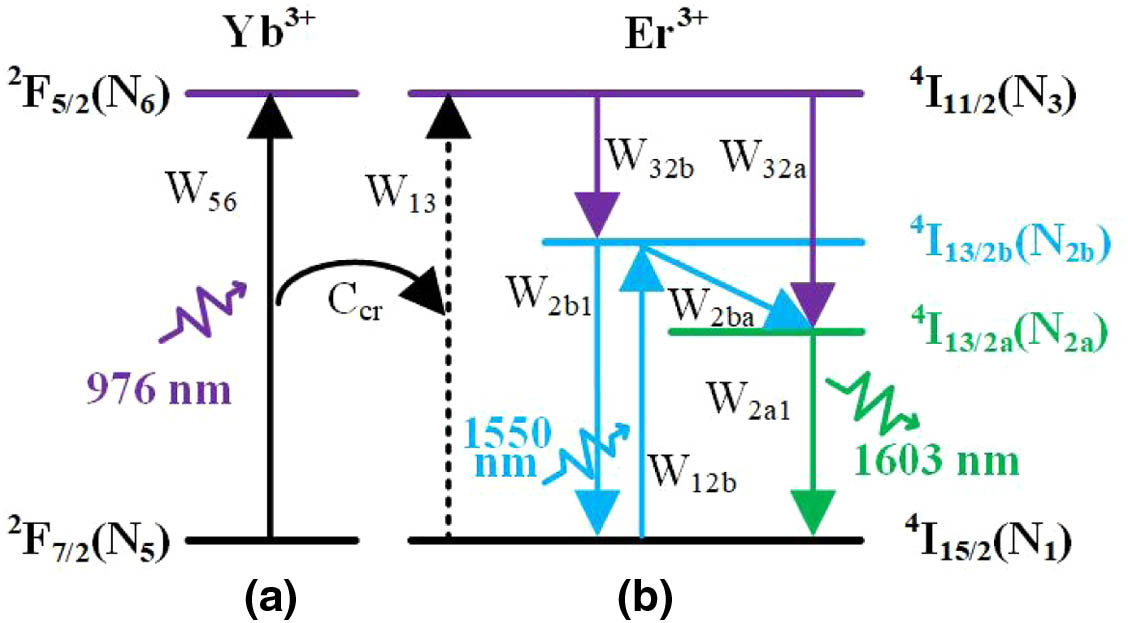
In this paper, a technique combining cascaded energy-transfer pumping (CEP) method and master-oscillator power-amplifier (MOPA) configuration is proposed for power scaling of 1.6-μm-band single-frequency fiber lasers (SFFLs), where the ion has a limited gain. The CEP technique is fulfilled by coupling a primary signal light at 1.6 μm and a C-band auxiliary laser. The numerical model of the fiber amplifier with the CEP technique reveals that the energy transfer process involves the pump competition and the in-band particle transition between the signal and auxiliary lights. Moreover, for the signal emission, the population density in the upper level is enhanced, and the effective population inversion is achieved thanks to the CEP. A single-frequency MOPA laser at 1603 nm with an output power of 52.6 W and an improved slope efficiency of 30.4% is experimentally obtained through the CEP technique. Besides, a laser linewidth of 5.2 kHz and a signal-to-auxiliary laser ratio of 60.7 dB are obtained at the maximum output power. The proposed technique is anticipated to be promising for increasing the slope efficiency and power scaling for fiber lasers operating at L band.
1 State Key Laboratory of High Field Laser Physics, Shanghai Institute of Optics and Fine Mechanics, Chinese Academy of Sciences, Shanghai 201800, China
2 Center of Materials Science and Optoelectronics Engineering, University of Chinese Academy of Sciences, Beijing 100049, China
3 CAS Center for Excellence in Ultra-intense Laser Science, Shanghai 201800, China
4 e-mail: yjpeng@siom.ac.cn
5 e-mail: lengyuxin@mail.siom.ac.cn
6 e-mail: ruxinli@mail.shcnc.ac.cn
A femtosecond mid-infrared optical vortex laser can be used for high harmonic generation to extend cutoff energy to the kilo-electron-volt range with orbital angular momentum, as well as other secondary radiations. For these, we demonstrate a high-energy femtosecond 4 μm optical vortex laser based on optical parametric chirped pulse amplification (OPCPA) for the first time. The optical vortex seed is generated from a femtosecond 4 μm laser by a silicon spiral phase plate with the topological charge of 1 before the stretcher. Through using a two-stage collinear OPCPA amplifier, the chirped vortex pulse is amplified to 12.4 mJ with 200 nm full width at half-maximum bandwidth. After compression, the vortex laser pulse with 9.53 mJ, 119 fs can be obtained. Furthermore, the vortex characteristics of the laser beam are investigated and evaluated. This demonstration can scale to generate a higher-peak-power vortex mid-IR laser and pave a new way for high field physics.
1 MOE Key Laboratory of Advanced Micro-Structured Materials, Shanghai 200092, China
2 Institute of Precision Optical Engineering, School of Physics Science and Engineering, Tongji University, Shanghai 200092, China
3 IFSA Collaborative Innovation Center, Shanghai Jiao Tong University, Shanghai 200240, China
Double-layer high-contrast subwavelength gratings that are separated by a dielectric space layer are investigated to achieve ultra-broadband reflection. The reflection phase of subwavelength gratings and the propagation phase shift between two gratings are manipulated to expand reflection bandwidth by properly stacking two reflective gratings. A reflector exhibiting a 99% reflectance bandwidth of in the near-infrared is designed. Then this reflector is prepared using laser interference lithography and ion beam planarization, and an ultra-broadband reflection is achieved with reflectance exceeding 97% over a wavelength range of 955 nm in the near-infrared region.


 Download:638次