1 Nanophotonics Research Center, Shenzhen Key Laboratory of Micro-Scale Optical Information Technology, Shenzhen University, Shenzhen 518060, China
2 Tianjin Union Medical Center, Tianjin 300121, China
3 e-mail: cjmin@szu.edu.cn
4 e-mail: xcyuan@szu.edu.cn
Tip-enhanced Raman scattering (TERS) spectroscopy is a nondestructive and label-free molecular detection approach that provides high sensitivity and nanoscale spatial resolution. Therefore, it has been used in a wide array of applications. We demonstrate a gap-plasmon hybridization facilitated by a bottom-illuminated TERS configuration. The gap-plasmon hybridization effect is first performed with the finite-difference time-domain method to optimize the parameters, and experiments are then conducted to calibrate the performance. The results demonstrate an enhancement factor of 1157 and a spatial resolution of 13.5 nm. The proposed configuration shows great potential in related surface imaging applications in various fields of research.
1 Centre de Nanosciences et Nanotechnologies (C2N), Université-Paris-Sud, CNRS UMR 9001, Université Paris-Saclay, Orsay 91405, France
2 Current address: Department of Materials Science and Engineering, Massachusetts Institute of Technology, Cambridge, Massachusetts 02139, USA
3 Institut des Sciences Analytiques et de Physico-Chimie pour l’Environnement et les Matériaux, CNRS, Université de Pau et des Pays de l’Adour, 64053 Pau Cedex, France
4 Laboratoire Charles Fabry, Institut d’Optique Graduate School, CNRS, Université Paris-Saclay, 91127 Palaiseau Cedex, France
5 Current address: LP2N, Institut d’Optique Graduate School, CNRS, Univ. Bordeaux, 33400 Talence, France
6 Department of Physics, Bridgewater State University, Bridgewater, Massachusetts 02325, USA
7 e-mail: laurent.vivien@c2n.upsaclay.fr
Nonlinear all-optical technology is an ultimate route for next-generation ultrafast signal processing of optical communication systems. New nonlinear functionalities need to be implemented in photonics, and complex oxides are considered as promising candidates due to their wide panel of attributes. In this context, yttria-stabilized zirconia (YSZ) stands out, thanks to its ability to be epitaxially grown on silicon, adapting the lattice for the crystalline oxide family of materials. We report, for the first time to the best of our knowledge, a detailed theoretical and experimental study about the third-order nonlinear susceptibility in crystalline YSZ. Via self-phase modulation-induced broadening and considering the in-plane orientation of YSZ, we experimentally obtained an effective Kerr coefficient of in an 8% (mole fraction) YSZ waveguide. In agreement with the theoretically predicted , the third-order nonlinear coefficient of YSZ is comparable with the one of silicon nitride, which is already being used in nonlinear optics. These promising results are a new step toward the implementation of functional oxides for nonlinear optical applications.
1 Nanophotonics Research Center, Shenzhen Key Laboratory of Micro-scale Optical Information Technology, Institute of Microscale Optoelectronics, Shenzhen University, Shenzhen 518060, China
2 School of Electrical and Electronic Engineering, Nanyang Technological University, Singapore 639798, Singapore
3 e-mail: ayst3_1415926@sina.com
4 e-mail: leiting@szu.edu.cn
The photonic spin Hall effect plays an important role in photonic information technologies, especially in on-chip spin Hall devices. However, conventional devices suffer from low efficiency or narrow bandwidth, which prevents their practical application. Here, we introduce a spin Hall device using inverse design to achieve both high efficiency and broadband. Spin-dependent light separation is enabled by a 2.4 μm circular device with 100 nm pixels. The photonic spin Hall element is fabricated on a silicon-on-insulator wafer compatible with a standard integrated photonic circuit. The spin light is detected and emitted with an efficiency of up to 22% and 35%, respectively, over a 200 nm bandwidth at optical wavelength.
We demonstrate 5 dB net gain in an erbium-doped tellurium-oxide-coated silicon nitride waveguide. The amplifier design leverages the high refractive index and high gain in erbium-doped tellurite glass as well as the ultra-low losses and mature, reliable, and low-cost fabrication methods of silicon nitride waveguide technology. We show that the waveguide platform demonstrates low background propagation losses of 0.25 dB/cm based on a ring resonator device with a factor of at 1640 nm. We measure 5 dB peak net gain at 1558 nm and of net gain across the C band in a 6.7 cm long waveguide for 35 mW of launched 1470 nm pump power. Gain per unit length of 1.7 and 1.4 dB/cm is measured in a 2.2 cm long waveguide for 970 and 1470 nm pump wavelengths, respectively. Amplifier simulations predict that gain can be achieved across the C band simply by optimizing waveguide length and fiber-chip coupling. These results demonstrate a promising approach for the monolithic integration of compact erbium-doped waveguide amplifiers on silicon nitride chips and within silicon-based photonic integrated circuits.
We propose what we believe is a novel optical thermometry strategy (FIR-Ex) based on the fluorescence intensity ratio (FIR) between two radiations associated with the same emission peak but different excitation wavelengths, in contrast to the traditional approach (FIR-Em), which depends on the FIR at varying emission wavelengths. The temperature-dependent FIR within the FIR-Ex strategy arises from the different charge/energy evolution routes, rather than the distribution of thermally coupled levels within the FIR-Em strategy. Considerable diversity in thermal behaviors and luminescence mechanisms was demonstrated by analyzing the 618 nm red emission in -doped congruent (Pr:CLN) under 360 and 463 nm excitations. The temperature sensitivity was further improved via codoping due to the optimization of charge dynamics and energy transfer processes. Given its wide detection scope, relatively high absolute sensitivity at low temperature, and high tunability of temperature sensitivity, the FIR-Ex strategy is promising for developing optical temperature-sensing materials with high performance.
1 Department of Applied Physics, East China Jiaotong University, Nanchang 330013, China
2 Faculty of Information Technology, College of Microelectronics, Beijing University of Technology, Beijing 100124, China
3 Center for Emergent Matter Science (CEMS), RIKEN, Wako, Saitama 351-0198, Japan
4 Key Laboratory of Low-Dimensional Quantum Structures and Quantum Control of Ministry of Education, Department of Physics and Synergetic Innovation Center for Quantum Effects and Applications, Hunan Normal University, Changsha 410081, China
5 Department of Physics, Zhejiang Sci-Tech University, Hangzhou 310018, China
6 e-mail: jinghui73@foxmail.com
7 e-mail: aixichen@zstu.edu.cn
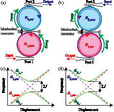
We propose to achieve nonreciprocal quantum control of photons in a quadratic optomechanical (QOM) system based on directional nonlinear interactions. We show that by optically pumping the QOM system in one side, the effective QOM coupling can be enhanced significantly in that side, but not for the other side. This, contrary to the intuitive picture, allows the emergence of a nonreciprocal photon blockade in such optomechanical devices with weak single-photon QOM coupling. Our proposal opens up the prospect of exploring and utilizing quantum nonreciprocal optomechanics, with applications ranging from single-photon nonreciprocal devices to on-chip chiral quantum engineering.
We propose a scheme to generate strong squeezing of a mechanical oscillator in an optomechanical system through Lyapunov control. Frequency modulation of the mechanical oscillator is designed via Lyapunov control. We show that the momentum variance of the mechanical oscillator decreases with time evolution in a weak coupling case. As a result, strong mechanical squeezing is realized quickly (beyond 3 dB). In addition, the proposal is immune to cavity decay. Moreover, we show that the obtained squeezing can be detected via an ancillary cavity mode with homodyne detection.
We demonstrate a high-energy all-fiber short wavelength gain-switched thulium-doped fiber laser for volumetric photoacoustic (PA) imaging of lipids. The laser cavity is constructed by embedding a short piece of gain fiber between a pair of fiber Bragg gratings (FBGs). Through using three pairs of FBGs with operation wavelengths at 1700, 1725, and 1750 nm, three similar lasers are realized with a cavity length of around 25 cm. Under a maximum pump energy of 300 μJ at 1560 nm, laser pulse energies of 58.2, 66.8, and 75.3 μJ are, respectively, achieved with a minimum pulse width of at a repetition rate of 10 kHz. Volumetric imaging of lipids is validated through scanning a fat beef slice with a PA microscopy system incorporated with the newly developed source, and a lateral resolution of 18.8 μm and an axial resolution of 172.9 μm are achieved. Moreover, the higher shooting speed of the developed source can potentially allow for increasing at twice the frame rate of current intravascular PA imaging.
1 Wuhan National Laboratory for Optoelectronics (WNLO) & National Engineering Laboratory for Next Generation Internet Access System, School of Optical and Electronic Information, Huazhong University of Science and Technology, Wuhan 430074, China
2 State Key Laboratory of Optical Fiber and Cable Manufacture Technology, Yangtze Optical Fiber and Cable Joint Stock Limited Company (YOFC) R&D Center, Wuhan 430073, China
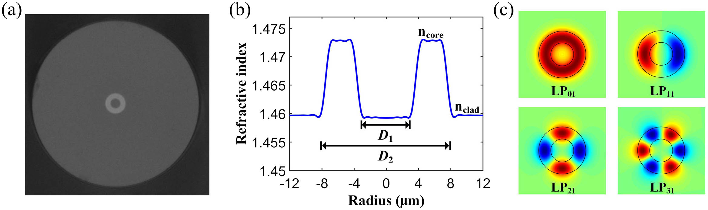
A theoretical and experimental study on curvature sensing using a Brillouin optical time-domain analyzer based on the ring-core fiber (RCF) is reported. The Brillouin gain spectrum of the RCF is investigated, and the Brillouin frequency shift (BFS) dependence on temperature and strain is calibrated. We theoretically analyze the fiber bending-induced BFS and peak Brillouin gain variation for the RCF through a numerical simulation method, and the RCF is revealed to have a high curvature sensitivity. Distributed curvature sensing is successfully demonstrated, with the bending radius ranging from 0.5 to 1.5 cm, corresponding to a BFS variation from 32.90 to 7.81 MHz. The RCF takes advantage of great bending loss resistance, and the maximum macrobending loss at the extreme bending radius of 0.5 cm is less than 0.01 dB/turn. Besides, the peak Brillouin gain of the RCF is discovered to vary significantly in response to fiber bending, which is expected to be another parameter for distributed curvature determination. The results imply that the RCF is a promising candidate for highly sensitive distributed curvature measurement, especially in sharp bending circumstances.
1 College of Science, Nanjing University of Aeronautics and Astronautics, Nanjing 210016, China
2 Key Laboratory for Intelligent Nano Materials and Devices (MOE), Nanjing University of Aeronautics and Astronautics, Nanjing 210016, China
3 e-mail: cxkan@nuaa.edu.cn
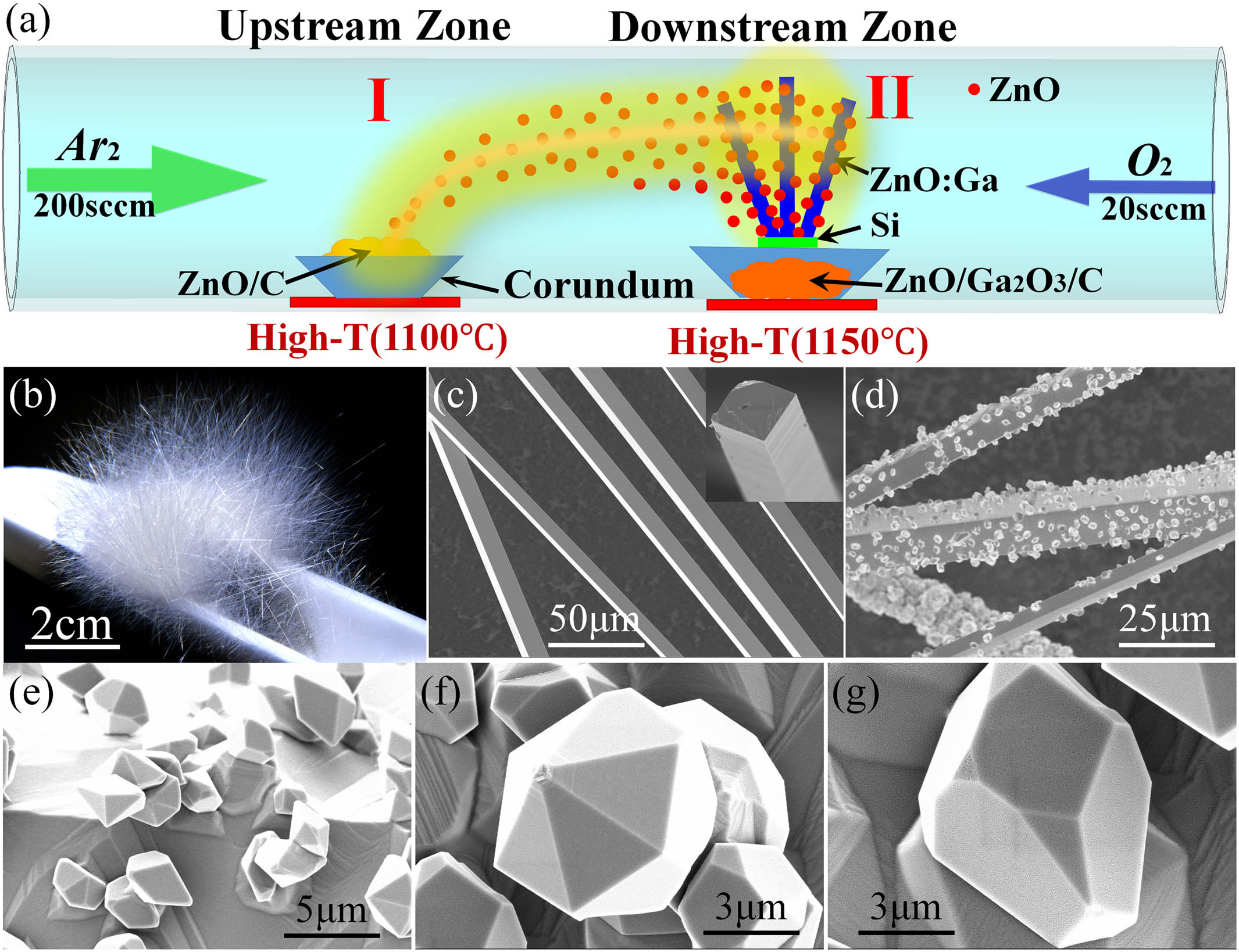
Due to their outstanding surface-to-volume ratio, highly smooth surface, and well-defined crystal boundary, semiconducting micro-/nanocrystals have been used as a pivotal platform to fabricate multifunctional optoelectronic devices, such as superresolution imaging devices, solar concentrators, photodetectors, light-emitting diodes (LEDs), and lasers. In particular, micro-/nanocrystals as key elements can be employed to tailor the fundamental optical and electronic transport properties of integrated hetero-/homostructures. Herein, ZnO microcrystal-decorated pre-synthesized Ga-doped ZnO microwire (ZnO@ZnO:Ga MW) was prepared. The single ZnO@ZnO:Ga MW can be used to construct optically pumped Fabry–Perot (F–P) mode microlasers, with the dominating lasing peaks centered in the violet spectral region. Stabilized exciton-polariton emissions from single ZnO@ZnO:Ga MW-based heterojunction diode can also be realized. The deposited ZnO microcrystals can facilitate the strong coupling of F–P optical modes with excitons, leading to the formation of exciton-polariton features in the ZnO@ZnO:Ga MW. Therefore, the waveguiding lighting behavior and energy-band alignment of ZnO microcrystal-sheathed ZnO:Ga MW radial structures should be extremely attractive for potential applications in semiconducting microstructure-based optoelectronic devices, such as micro-LEDs, laser microcavities, waveguides, and photodetectors.
1 Department of Materials Science & Engineering, Massachusetts Institute of Technology, Cambridge, Massachusetts 02139, USA
2 Department of Electrical and Computer Engineering, University of Washington, Seattle, Washington 98195, USA
3 Department of Physics, University of Washington, Seattle, Washington 98195, USA
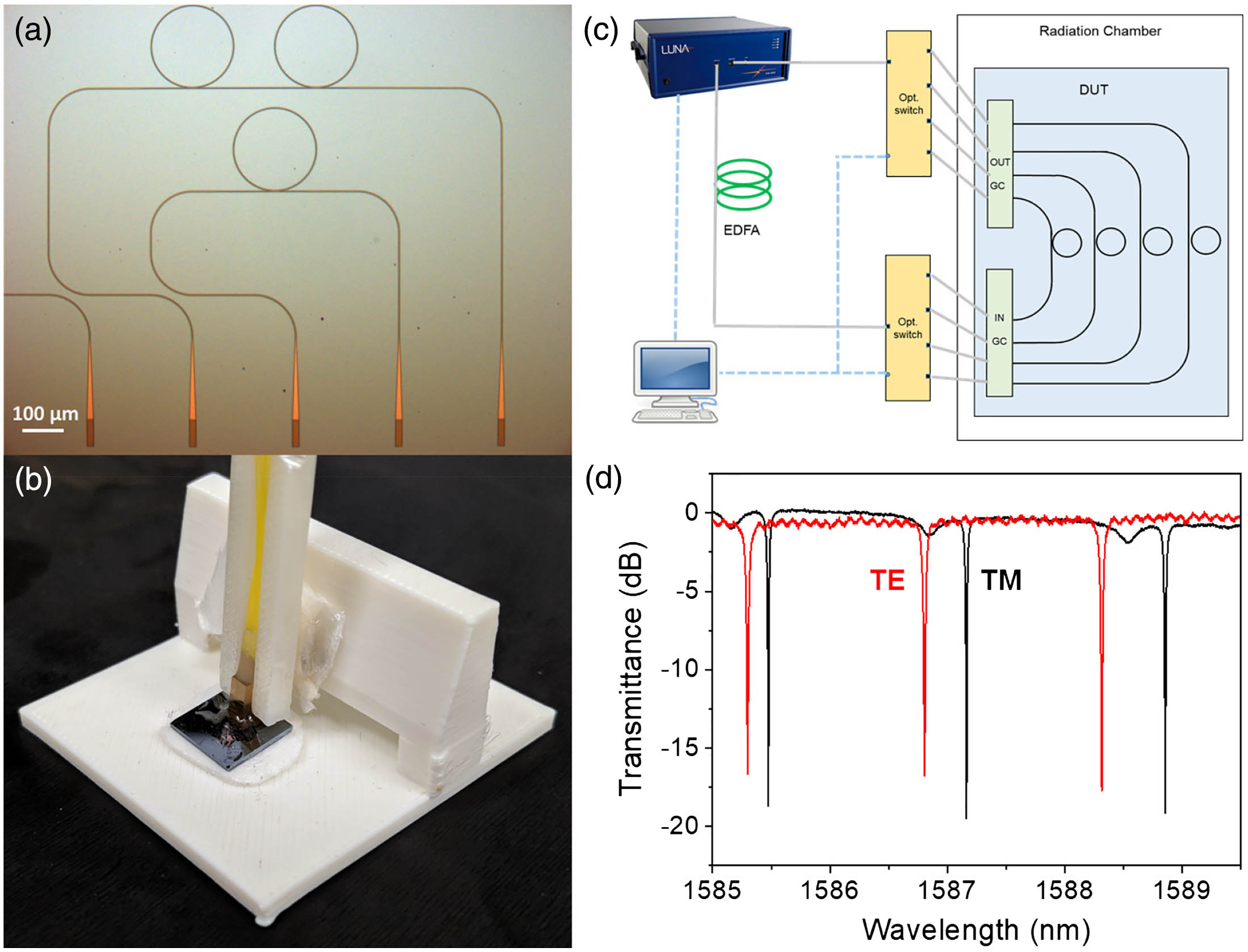
Integrated photonics is poised to become a mainstream solution for high-speed data communications and sensing in harsh radiation environments, such as outer space, high-energy physics facilities, nuclear power plants, and test fusion reactors. Understanding the impact of radiation damage in optical materials and devices is thus a prerequisite to building radiation-hard photonic systems for these applications. In this paper, we report real-time, in situ analysis of radiation damage in integrated photonic devices. The devices, integrated with an optical fiber array package and a baseline-correction temperature sensor, can be remotely interrogated while exposed to ionizing radiation over a long period without compromising their structural and optical integrity. We also introduce a method to deconvolve the radiation damage responses from different constituent materials in a device. The approach was implemented to quantify gamma radiation damage and post-radiation relaxation behavior of -cladded SiC photonic devices. Our findings suggest that densification induced by Compton scattering displacement defects is the primary mechanism for the observed index change in SiC. Additionally, post-radiation relaxation in amorphous SiC does not restore the original pre-irradiated structural state of the material. Our results further point to the potential of realizing radiation-hard photonic device designs taking advantage of the opposite signs of radiation-induced index changes in SiC and .
1 Department of Materials Science and Engineering, Massachusetts Institute of Technology, Cambridge, Massachusetts 02139, USA
2 Department of Biological Engineering, University of Delaware, Newark, Delaware 19716, USA
3 Key Laboratory of 3D Micro/Nano Fabrication and Characterization of Zhejiang Province, School of Engineering, Westlake University, Hangzhou 310024, China
4 Institute of Advanced Technology, Westlake Institute for Advanced Study, Hangzhou 310024, China
5 College of Optics & Photonics, University of Central Florida, Orlando, Florida 32816, USA
6 College of Information Science and Electronic Engineering, Zhejiang University, Hangzhou 310027, China
7 e-mail: xjia@udel.edu
8 e-mail: hujuejun@mit.edu
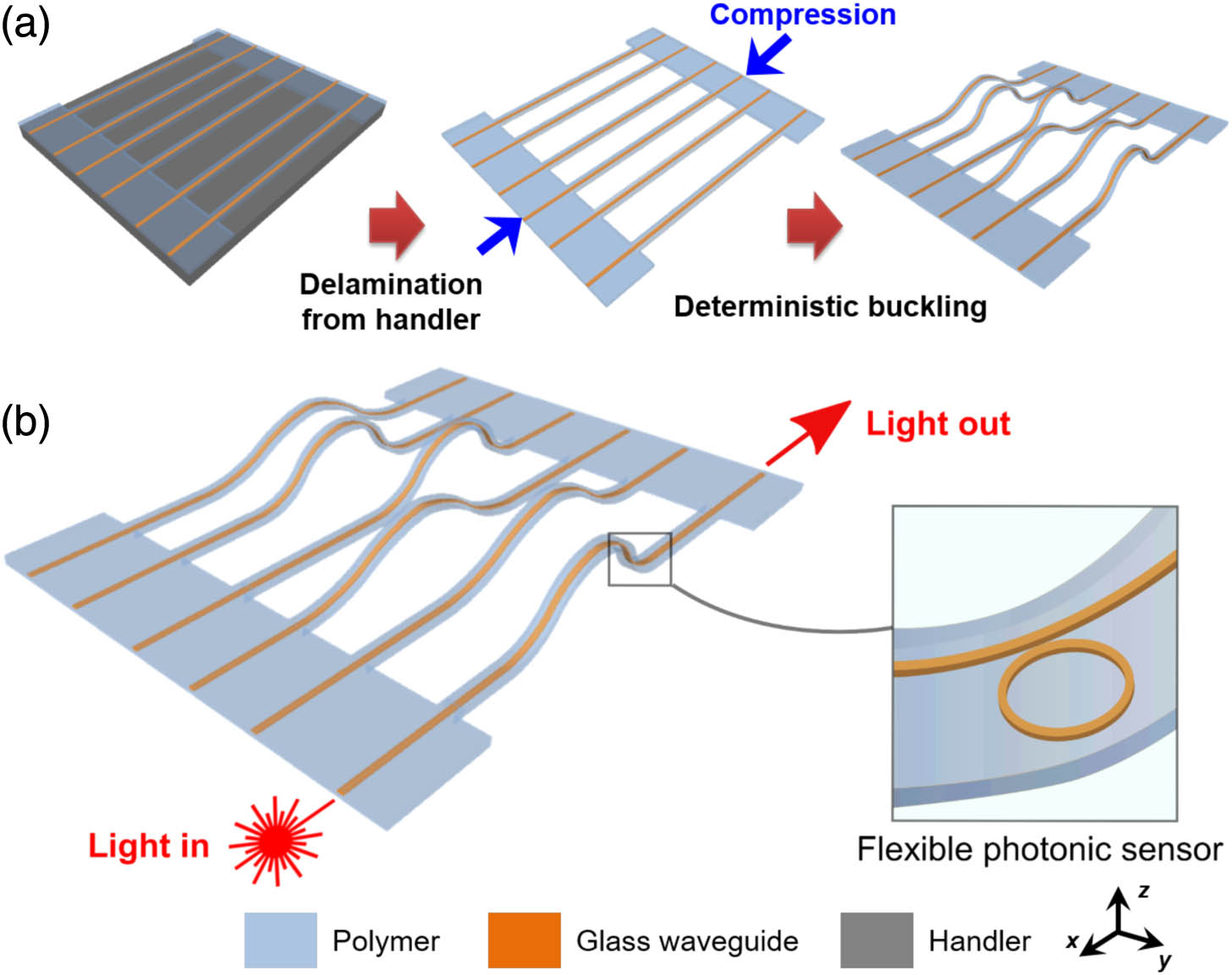
3D photonics promises to expand the reach of photonics by enabling the extension of traditional applications to nonplanar geometries and adding novel functionalities that cannot be attained with planar devices. Available material options and device geometries are, however, limited by current fabrication methods. In this work, we pioneer a method that allows for placement of integrated photonic device arrays at arbitrary predefined locations in 3D using a fabrication process that capitalizes on the buckling of a 2D pattern. We present theoretical and experimental validation of the deterministic buckling process, thus demonstrating implementation of the technique to realize what we believe to be the first fully packaged 3D integrated photonics platform. Application of the platform for mechanical strain sensing is further demonstrated.
1 Department of Physics and Astronomy, University of New Mexico, Albuquerque, New Mexico 87131, USA
2 Center for High Technology Materials, University of New Mexico, Albuquerque, New Mexico 87106, USA
3 Department of Electrical and Computer Engineering, University of New Mexico, Albuquerque, New Mexico 87131, USA
Recent advances in power scaling of fiber lasers are hindered by the thermal issues, which deteriorate the beam quality. Anti-Stokes fluorescence cooling has been suggested as a viable method to balance the heat generated by the quantum defect and background absorption. Such radiation-balanced configurations rely on the availability of cooling-grade rare-earth-doped gain materials. Herein, we perform a series of tests on an ytterbium-doped (ZBLAN) optical fiber to extract its laser-cooling-related parameters and show that it is a viable laser-cooling medium for radiation balancing. In particular, a detailed laser-induced modulation spectrum test is performed to highlight the transition of this fiber to the cooling regime as a function of the pump laser wavelength. Numerical simulations support the feasibility of a radiation-balanced laser, but they highlight that practical radiation-balanced designs are more demanding on the fiber material properties, especially on the background absorption, than solid-state laser-cooling experiments.
1 Photonics Research Group, Department of Information Technology, Ghent University-IMEC, 9052 Ghent, Belgium
2 Center of Nano and Biophotonics, Ghent University, 9052 Ghent, Belgium
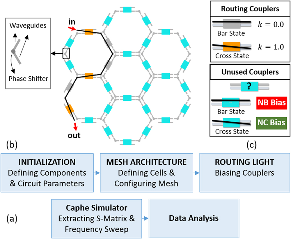
We present a study of the effect of imperfections on the transmission and crosstalk in programmable photonic meshes with feedback loops consisting of tunable couplers and phase shifters. The many elements in such a mesh can generate a multitude of parasitic paths when the couplers and phase shifters deviate even slightly from their nominal value. Performing Monte Carlo simulations, we show that small stochastic imperfections in the phase and coupling () can introduce unwanted interferences and resonances and significantly deteriorate the frequency response of the circuit. We also demonstrate that, in the presence of imperfections, the programming strategy of the unused couplers can reduce effects of such parasitics.
1 Department of Electrical and Computer Engineering, University of California, San Diego, California 92093, USA
2 King Abdulaziz City for Science and Technology (KACST), Riyadh 11442, Saudi Arabia
3 e-mail: fainman@ece.ucsd.edu
We report an advanced Fourier transform spectrometer (FTS) on silicon with significant improvement compared with our previous demonstration in [Nat. Commun.9, 665 (2018)2041-1723]. We retrieve a broadband spectrum (7 THz around 193 THz) with 0.11 THz or sub nm resolution, more than 3 times higher than previously demonstrated [Nat. Commun.9, 665 (2018)2041-1723]. Moreover, it effectively solves the issue of fabrication variation in waveguide width, which is a common issue in silicon photonics. The structure is a balanced Mach–Zehnder interferometer with 10 cm long serpentine waveguides. Quasi-continuous optical path difference between the two arms is induced by changing the effective index of one arm using an integrated heater. The serpentine arms utilize wide multi-mode waveguides at the straight sections to reduce propagation loss and narrow single-mode waveguides at the bending sections to keep the footprint compact and avoid modal crosstalk. The reduction of propagation loss leads to higher spectral efficiency, larger dynamic range, and better signal-to-noise ratio. Also, for the first time to our knowledge, we perform a thorough systematic analysis on how the fabrication variation on the waveguide widths can affect its performance. Additionally, we demonstrate that using wide waveguides efficiently leads to a fabrication-tolerant device. This work could further pave the way towards a mature silicon-based FTS operating with both broad bandwidth (over 60 nm) and high resolution suitable for integration with various mobile platforms.


 Download:658次