红外与激光工程, 2020, 49 (9): 20201039, 网络出版: 2021-01-04
从亚波长光栅到超构光栅:原理、设计及应用  下载: 2120次
From subwavelength grating to metagrating: principle, design and applications
图 & 表
图 1. 不同尺度下的介质光栅。(a)衍射光栅; (b)共振(亚波长)光栅;(c)等效介质薄膜
Fig. 1. Dielectric grating at different scales. (a) Diffraction gratings; (b) Resonant (subwavelength) gratings; (c) Equivalent dielectric films
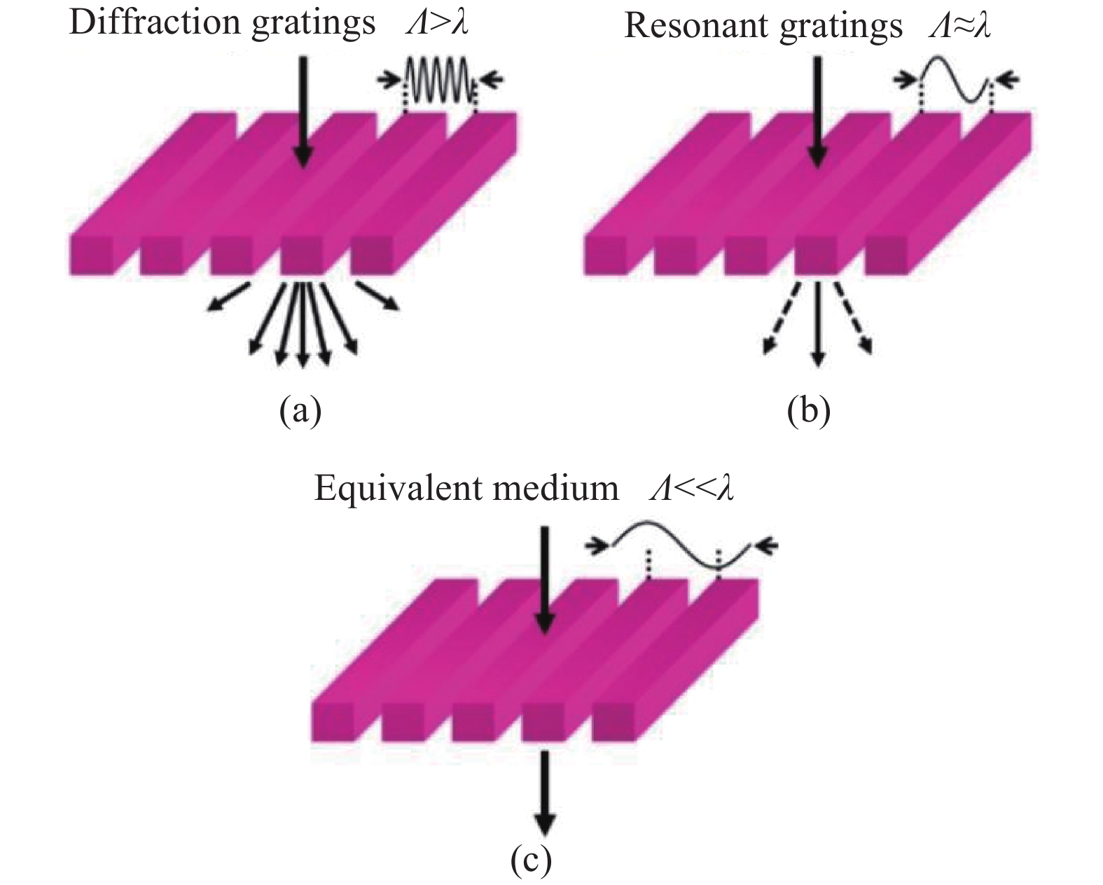

图 3. 不同波段的亚波长光栅和超构光栅[17-27]
Fig. 3. Subwavelength gratings and metagratings at different wavelengths[17-27]

图 4. 级联超构光栅实现的窄带窄角透射滤波器结构及其透射谱[28]
Fig. 4. Narrow-frequency sharp-angular transmission filter structures and the spectrum using cascaded metagratings[28]

图 5. 光栅分析理论:模式展开、共振与干涉。(a)耦合模理论[31];(b)导模共振理论[33-34];(c)广义Kerker效应[35]
Fig. 5. Analytical theory of optical gratings: mode expansion, resonant and interference. (a) Coupled-mode theory[31]; (b) Guided-mode resonance theory[33-34] ; (c) Generalized Kerker effect[35]


图 7. 电路型超构光栅衍射调控[45-46]
Fig. 7. Electrical circuits type of metagrating diffraction modulation[45-46]


图 10. 矩形介质光栅实现高效率光束偏折[50]
Fig. 10. High efficient beam-steering using rectangle dielectric grating[55,50]

图 11. (a)具有纳米级结构和逐点测量传感功能的微流控芯片示意图[78];一次性导模共振生物传感器芯片的 (b) 示意图和(c)其光学图像,包括在环烯烃共聚物(COC)基板上的亚波长光栅(一维TiO2光栅)结构和用于处理注射液的微流体模块[80]
Fig. 11. (a) Schematic of microfluidic chip with nanostructured and spot-wise functionalized sensor field[78]; (b) Schematic and (c) optical image of the disposable GMR biosensor chip, consisting of a subwavelength grating (a one-dimensional TiO2 grating structure) on a cyclic olefin copolymer substrate and a microfluidic module for handing the injection of fluid sample into the sensing area[80]

图 12. 纳米孔阵列亚波长光栅滤光片。(a) 基于金属铝的纳米孔阵列滤光片,尺寸边长分别为 (a1) 10 μm,(a2) 5 μm,(a3) 2.4 μm,(a4) 1.2 μm的滤光片光谱[87];(b)纳米孔阵列形成的彩色徽标[88];(c)与CMOS图像传感器结合的纳米孔阵列滤光片[89];(d)基于硅材料亚波长光栅滤光片[90]
Fig. 12. Nanohole array subwavelength grating filters. (a) Transmission spectra of the hole array filters with different side length (a1) 10 μm, (a2) 5 μm, (a3) 2.4 μm, (a4) 1.2 μm[87]; (b) Color logo based on the nanohole array filter[88]; (c) oNanohle array filter integrated with CMOS imaging sensor[89] ; (d) Si subwavelength grating color filters[90]

图 13. 一维纳米光栅滤光片。超薄银等离子体纳米光栅滤光片(a)结构示意图和(b)光谱图[98];(c) 纳米光栅滤光片结构示意图;(d) 颜色光谱与滤光片光栅周期之间的关系[100]
Fig. 13. One dimensional nanograting color filters. (a) Schematic diagram and (b) the spectra of the ultrathin Ag nanogratings color filters[98];(c) Schematic diagram of the nanograting color filters; (d) Relationship between color spectra and period of the color filter nanograting[100]

图 14. 硅纳米线阵列滤光片扫描电子显微镜图。(b) 不同纳米线阵列的滤光片反射光谱[105];(c) 垂直硅纳米线光电探测器的概念示意图;(d) 硅纳米线阵列拍摄测试对象的彩色图像[106]
Fig. 14. (a) SEM images of silicon nanowire array; (b) Reflection spectra of color filter for different nanowire arrays[105]; (c) Concept schematic of photoelectric detectors based on vertical silicon nanowires; (d) Color image of test objects taken by silicon nanowire arrays[106]

图 15. (a) 硅铝杂化纳米盘滤光片;(b) 硅铝杂化纳米盘减色滤光片的反射光谱[108];(c)十字形硅纳米天线阵列滤光片;(d)十字形硅纳米天线阵列透射光谱[113]
Fig. 15. (a) Schematic configuration and (b) reflection spectral responses of the subtractive CMY color filters incorporating a Si-Al hybrid-ND metasurface formed on a Si substrate[108]; (c) Cross-shaped Si nanoantennas color filters and (d) its transmittance spectra[113]

图 16. 亚波长光栅(各向异性超材料薄膜)(a)结构图及(b)吸收谱图[118];(c) MICM结构示意图;(d)不同结构的吸收谱对比图[119]
Fig. 16. (a) Diagram and (b) absorption spectra of the subwavelength grating (sawtooth anisotropic metamaterial thin film)[118]; (c) Diagram of MICM (metal-insulator composite multilayer); (d) Comparison of absorption spectra for different structures[119]

图 17. (a)纳米盘单元亚波长光栅吸收谱[123];(b) 纳米盘单元亚波长光栅电磁场强度和能量损失图[123]; (c) 多层金属−介质−金属谐振堆栈结构亚波长光栅吸收器吸收谱图[131];(d) Ti-SiO2-Al 结构构成的亚波长光栅太阳能吸收薄膜[133]
Fig. 17. (a)Absorption spectra of subwavelength grating with nanodisk unit[123]; (b) Field intensity and energy loss of subwavelength grating with nanodisk unit[123]; (c) Absorption spectra of subwavelength grating absorber with multilayered metal-dielectric-metal resonant stacks [131]. (d) Subwavelength grating of Ti-SiO2-Al structure for solar energy absorption film[133]

图 18. (a)不同参数的 Ag-SiO2-Ag 十字形结构的亚波长光栅结构的吸收谱图[135]; (b)梯形阵列结构亚波长光栅及其消光谱[139]; (c)环形阵列结构及其吸收谱[140]; (d) 锥形亚波长光栅吸收器吸收谱[145]
Fig. 18. (a) Measured absorption spectra of fabricated Ag-SiO2-Ag cross structure of subwavelength grating with different parameters[135]; (b) Extinction spectra using crossed trapezoid array subwavelength metagraing[139]; (c) Absorption spectra of ring array structure[140]; (d) Absorption spectra of subwavelength grating of cone unit structure[145]


陈瑞, 柳夏, 王虹, 石伟怡, 刘伟男, 江绍基, 董建文. 从亚波长光栅到超构光栅:原理、设计及应用[J]. 红外与激光工程, 2020, 49(9): 20201039. Rui Chen, Xia Liu, Hong Wang, Weiyi Shi, Weinan Liu, Shaoji Jiang, Jianwen Dong. From subwavelength grating to metagrating: principle, design and applications[J]. Infrared and Laser Engineering, 2020, 49(9): 20201039.


 PDF全文
PDF全文
