Chinese Optics Letters, 2015, 13 (3): 031401, Published Online: Sep. 25, 2018  

Metamorphic growth of 1.55  μm InGaAs/InGaAsP multiple quantum wells laser structures on GaAs substrates

Author Affiliations
1 Institute of Information Photonics and Optical Communications, Beijing University of Posts and Telecommunications (BUPT); State Key Laboratory of Information Photonics and Optical Communications (BUPT), Beijing 100876, China
2 Key Laboratory of Semiconductor Materials Science, Institute of Semiconductors, Chinese Academy of Sciences, Beijing 100083, China
Abstract
We fabricate a GaAs-based InGaAs/InGaAsP multiple quantum wells (MQWs) laser at 1.55 μm. Using two-step growth method and thermal cyclic annealing, a thin low-temperature InP layer and a thick InP buffer layer are grown on GaAs substrates by low-pressure metal organic chemical vapor deposition technology. Then, high-quality MQWs laser structures are grown on the InP buffer layer. Under quasi-continuous wave (QCW) condition, a threshold current of 476 mA and slope efficiency of 0.15 mW/mA are achieved for a broad area device with 50 μm wide strip and 500 μm long cavity at room-temperature. The peak wavelength of emission spectrum is 1549.5 nm at 700 mA. The device is operating for more than 2000 h at room-temperature and 600 mA.

Long-wavelength (1.55 or 1.31 μm) semiconductor lasers are the essential devices in the fiber communication systems. InP-based optoelectronic devices are essential for optical communication and have shown great potential for long-distance fiber communication, such as lasers and detectors[1,2]. Most of commercial 1.55 μm semiconductor lasers are InP-based InGaAsP lasers. Unsatisfactorily, some insufficient of InP substrates, such as high cost and frailness, limit some applications in several areas (large area integrated devices)[3,4]. GaAs substrates have many good performances, such as relatively low cost and good mechanical properties, which can make up for the inadequacy of InP substrates. Moreover, GaAs-based integrated circuit (IC) technology is relatively mature in comparison with that of InP-based IC[5,6]. If GaAs electronic devices and InP-related optoelectronic devices are combined with GaAs substrates, optoelectronic ICs could be realized easily, and the optical fiber communication systems can be made an important progress[6]. Therefore, the technology of growth high-quality InP-based epilayers on GaAs substrates have been attracted considerable attention recently[7,8].

However, a large number of threading dislocations will appear when InP layers are directly grown more than 5 nm thick on GaAs substrates under normal growth conditions, because there is 3.8% lattice mismatch of InP/GaAs heterostructure[8,9]. In order to obtain high-quality InP epilayers on GaAs substrates for devices, the two-step growth method, thermal cyclic annealing (TCA) and strained-layer superlattice (SLS) are widely used[3,7,8,10]. In 1991, Kimura et al. fabricated a 1.3 μm InGaAsP/InP quantum well (QW) laser and a PIN photodiode (PD) on GaAs substrates[11]. In our previous work, we have completed some works on metamorphic growth of InP epilayers on GaAs substrates by using two-step growth method, TCA and SLS. In 2007, we grew high-quality InP epilayers on GaAs substrates, in which the full-widths at half-maximum (FWHM) of X-ray diffraction (XRD) ω scans were 219 arcsec for a 2.6 μm thick heteroepitaxial InP[8,12]. In 2009, we successfully fabricated a PIN PD on GaAs substrate and the quantum efficiency of the PD was 67.3% at 1549.5 nm[13]. In 2014, we fabricated a high-efficiency dual-absorption InGaAs/InP PD on GaAs substrates, in which the quantum efficiency was 64% at a wavelength of 1522 nm, beside, the 3 dB bandwidth was 26 GHz[14].

At present, four approaches are used for 1.55 μm range GaAs-based lasers. The first one is InP/GaAs wafer bonding technology. The device is based on fusion of the InGaAsP active layer grown on InP substrates and the AlGaAs Bragg reflectors grown on GaAs substrates[15,16]. But, this technology is too complex and difficult to be used to produce diode lasers with low-cost[17]. The second one is growth of GaInNAsSb QW laser materials on GaAs substrate[18,19], while the peak wavelength was not easy to control. The third one is to use In(Ga)As/GaAs quantum dots (QDs) as the active region[20,21]. The fourth one is to use InGaAs/GaAs QW as the active region which is grown on metamorphic InGaAs layers deposited on GaAs substrates[22]. Both QDs and QW lasers have common insufficient that the peak wavelength of spectrum is not strictly 1.55 μm. To avoid these problems, we propose a method that direct growth of 1.55 μm InP-based laser structures on GaAs substrates to compensate for the lack of complex technology and uncontrolled wavelength.

In this Letter, we report metamorphic growth of 1.55 μm InGaAs/InGaAsP multiple QWs (MQWs) laser structures on GaAs substrates by low-pressure (LP) metal organic chemical vapor deposition (MOCVD) technology. The laser structures were grown on GaAs substrates by two-step growth method in which we had optimized the growth temperature, growth rate and V/III ratio[12]. The GaAs-based laser structures were characterized by double crystal XRD (DC-XRD), room-temperature (RT) photoluminescence (PL), atomic force microscopy (AFM), transmission electron microscopy (TEM) and electrochemical current-voltage (ECV). The test results show that the quality of epilayers is satisfactory and the epitaxial materials can be used to fabricate devices. A broad area laser emitter with 50 μm strip was fabricated and the pulse wave threshold current of the device is 476 mA at RT. Multi-longitudinal mode with a peak wavelength of 1549.5 nm is presented and FWHM of the envelope is 4.9 nm when the injection current is 700 mA. Under auto-current-control (ACC) mode, the diode laser had been operated for more than 2000 h at 600 mA and RT.

The epitaxial layers were grown by LP-MOCVD system on a n-type GaAs substrate. The pressure of the reactor chamber was 100 Torr. The 2 inch (100) oriented GaAs wafers were used as the substrates. The source materials were trimethyl-indium, trimethyl-gallium, arsine and phosphine. Silane and diethylzinc were used as the precursors of p-dopants and n-dopants, respectively. Palladium-diffused H2 was used as the carrier gas and the flow rate was about 12 L/min.

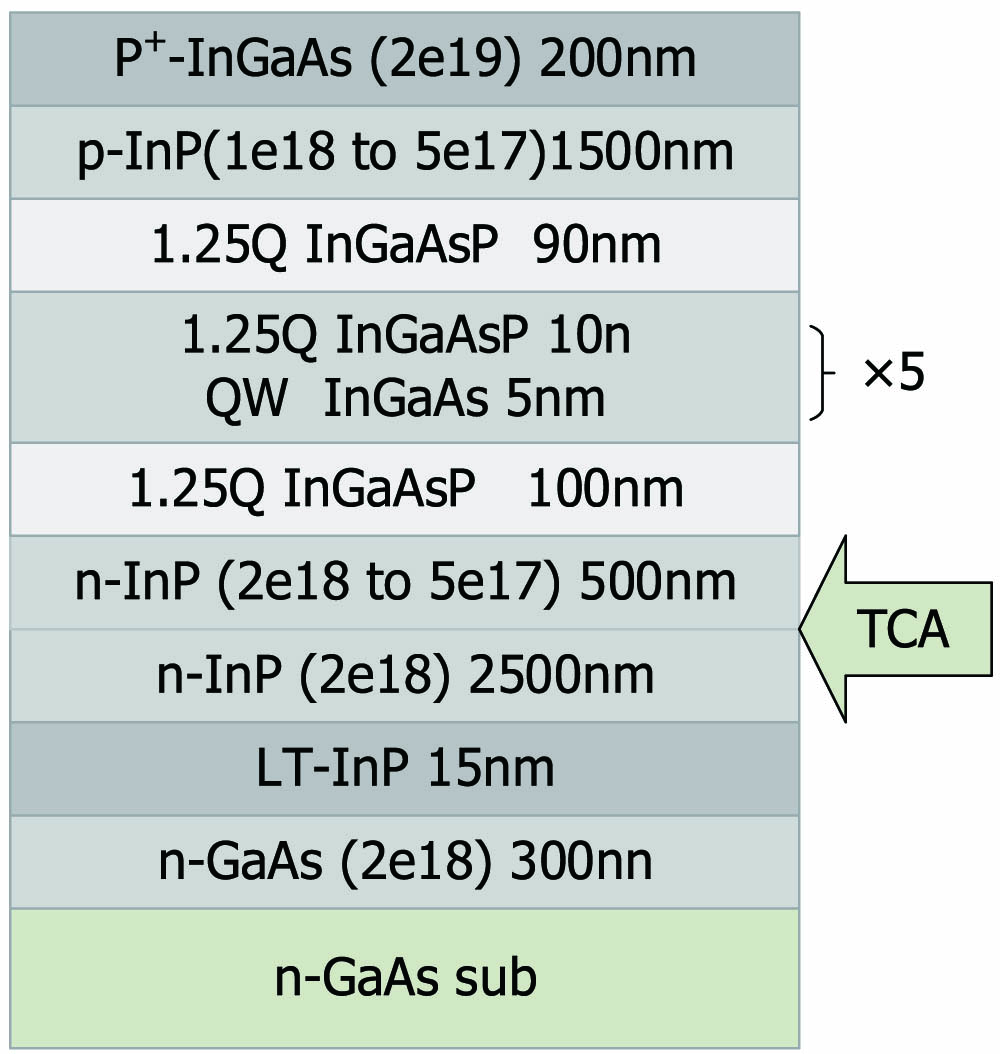
Figure 1 shows the structures schematic and growth process of the laser epilayers. At first, 300 nm thick GaAs layer was grown on n-type GaAs (100) substrates and the growth temperature was 720°C. Then, the substrates were cooled down to 450°C, 15 nm thick low-temperature InP layer was grown on the GaAs buffer layer, and the V/III ratio was 200. Additionally, the substrates were heated up to 655°C, a 2500 nm InP buffer layer was grown. After the growth, under the aegis of the phosphine, thermal cycle annealing was performed. The wafers were heated up to 700°C for 500 s, then cooled down to 300°C for each cycle. This procedure was repeated three times. Finally, InGaAs/InGaAsP MQWs structures were grown on the InP buffer layer. The active layers consisted of five periods of 5 nm lattice-matched In0.53Ga0.47As QWs and 10 nm 1.25Q lattice-matched InGaAsP barriers (band-gap wavelength: 1.25 μm)[23]. The active layers were sandwiched between 90 and 100 nm 1.25Q lattice-matched InGaAsP waveguide layers. Also, we grew the same laser epitaxial structures on InP substrates as a comparison.

Fig. 1. Structures schematic of laser epilayers and growth process on GaAs substrates.

下载图片 查看所有图片

The DC-XRD spectra (solid line) of the epitaxial structure are shown in Fig. 2. The FWHM of the rocking curve is 207 arcsec, in which FWHM of the epitaxial layers is relatively small and reflects the high crystalline quality of layers. The satellite peaks of the InGaAs/InGaAsP MQWs could be observed in the left and right sides of InGaAsP/InP epilayers peak. The dummy line of the Fig. 2 shows the rocking curve of MQWs laser on InP substrate. After removing the p+-InGaAsP layer and part of the p-InP cladding layer of the wafer by using wet chemical etching, we measured the PL spectrum of the sample at RT. As shown in inset of Fig. 2, the peak wavelength and the FWHM of the spectrum are 1539 and 77 nm, respectively.

Fig. 2. Rocking curve (ω2θ scan) of MQWs laser on GaAs substrate (solid line) and on InP substrate (dotted line) in the GaAs (004) reflection. Inset shows RT PL photoluminescence spectrum of MQWs for InP/GaAs laser after removing the surface layers.

下载图片 查看所有图片

The carrier concentration of the InP/GaAs laser materials was measured by ECV. Figure 3 shows the carrier concentration profiles. The hole concentration and electron concentration are 1×10¹⁸ and 2×1018cm3 in p-type and n-type InP cladding layers. The carrier concentration decreases rapidly in the InGaAsP waveguide layers, meanwhile the n-type carrier concentration of the MQWs region is about 2×1016cm3. As presented in the inset of Fig. 3, the hole concentration of 2×1019cm3 is obtained in the p+-InGaAs contact layer.

Fig. 3. Measured carrier concentration profiles of MQWs InP/GaAs laser material by ECV. Inset shows the hole concentration of p-type contact layer and part of cladding layer.

下载图片 查看所有图片

Fig. 4. (a) Cross-sectional TEM images of epilayers on GaAs substrate; (b) TEM images of active regions and (c) TEM images of active regions with dislocations.

下载图片 查看所有图片

Surface morphology of the wafers was investigated by AFM. The root mean square (RMS) surface roughnesses of 5 μm think laser structure, as measured by AFM over 10μm×10μm, is 1.35 nm. The surface of the wafers is smooth compare with other lasers that metamorphic growth laser on GaAs substrates[22]. TEM measurements were made to study the dislocations in the InP layers on the GaAs substrate. As shown in Fig. 4, there are many dislocations in the InP/GaAs interface. Much less propagation of dislocations through the buffer to the active regions, and most dislocations have either glided or annihilated when they penetrated to the active regions during the TCA step in the middle of the epitaxial growth. However, it is not that all dislocations are glided or annihilated, and there are also a few dislocations though the active regions [as shown in Fig. 4(c)]. To further analysis of dislocation density, etch pit density (EPD) of metamorphic InP/GaAs have been comprehensively studied and analyzed. First, the InGaAs layer of the epilayers surface was removed by H2SO4H2O2H2O(=1110), and InP layer was appeared. The InP layer surface morphologies observed by scanning electron microcopy (SEM) were very smooth. Thus, it could be used for EPD measurement. During EPD measurement, the etching was performed in H3PO4HBr(=21) solution (Huber etchant) at temperatures about 20°C and for duration 75 s about 700 nm deep. By calculating, the EPD of InP layer is about 4×106cm2.

A 50 μm strip carved by conventional photolithography was used as P-contact metallization (Ti-Pt-Au). After substrate thinning and polishing, N-metallization (Au-Ge-Ni) was deposited onto the bottom side of the wafer. The wafer was cleaved (200μm×500μm) and separated into individual chips. Then, the chip was made into a single laser emitter on Cu heat sinks, as shown in the Fig. 5. The inset of Fig. 5(b) shows single ship of the single emitter laser.

Fig. 5. (a) Schematic structures of the device with 50 μm strip. (b) A single emitter laser. Inset shows the individual chip of the laser diode.

下载图片 查看所有图片

The device characteristics were measured under quasi-continuous wave condition with a pulse width of 5 μs and a repetition rate of 1 kHz. Figure 6 shows the output power and voltage versus injection current. The threshold current density and the single side slope efficiency are 1.9kA/cm2 and 0.14 mW/mA, respectively. As comparison, the threshold current density and the single side slope efficiency of the laser on InP substrate are 900A/cm2 and 0.15 mW/mA. Because there are high-density threading dislocations in the buffer layers, the crystalline quality of laser structures on GaAs substrates is poor compare with laser structures on InP substrates. The threshold current density of laser on GaAs substrates is two times larger than that on InP substrates. But their single side slope efficiency is almost the same. We suspect that dislocations of metamorphic growth InP layers on GaAs substrates mainly influence the threshold current. We think that there are two points for discussing. First, the fast stimulated emission does not allow the carriers to recombine via non-radiative pathways since above laser threshold. Secondly, the proportion of nonradiative recombination is very small at the early work of device, and it has not obvious influence on the slope efficiency. When the injection current is 400 mA, the spectrum of device is shown in inset (a) of Fig. 6. As shown in inset (b) of Fig. 6, multi-longitudinal mode with a peak wavelength of 1549.5 nm is presented and FWHM of the envelope is 4.9 nm when the injection currents is 700 mA. The metamorphic lasers which are grown on metamorphic InGaAs layers deposited on GaAs substrates have a lower threshold current density compare to the InP laser that is grown on GaAs substrate. But the spectrum peak wavelength of InP laser on GaAs substrate is more easy to achieve 1.55 μm compare to the metamorphic lasers which are grown on InGaAs layers deposited on GaAs substrates. The vertical far field distribution of our device has a nearly Gaussian shape with a divergence angle of 39° (FWHM) which is shown in Fig. 7.

Fig. 6. Typical curves of output power and voltage versus injection current for the emitter laser at RT. The threshold current is 476 mA. Inset (a) shows optical spectrum taken at 400 mA. Inset (b) shows optical spectrum taken at 1.5-times threshold (700 mA). The ordinate values of the Inset (a) and Inset (b) are normalized intensity.

下载图片 查看所有图片

Fig. 7. Vertical far field distribution of the device at 700 mA.

下载图片 查看所有图片

The aging test has been made in the ACC mode with a driving current of 600 mA at RT as shown in Fig. 8. The laser had been operated for more than 2000 h, and carried out 7.8×10⁹ pulses lasing. The device observes 10% of degradation in the first 50 h, then, observes slowly degradation in the remaining hours. Thus, it shows that the metamorphic growth of InGaAs/InGaAsP MQWs on GaAs technique is a promising alternative for GaAs-based telecommunication lasers device. In the future work, we well dedicated to the study of optimize the buffer layers and the active regions, so that the devices achieve practical.

Fig. 8. Light-output power at RT and 600 mA as a function of time during the ACC aging tests with a driving current of 600 mA. Inset shows the aging test in the first 200 h.

下载图片 查看所有图片

In conclusion, the 1.55 μm InGaAs/InGaAsP MQWs laser structures are grown on n-type GaAs substrates by using two-step grown method and TCA. The XRD, TEM, AFM and ECV profiles show that the epitaxial materials could be used to fabricate devices. A broad area emitter laser with 50 μm strip is fabricated. The RT threshold current density of device is 1.9kA/cm2 and the slope efficiency is 0.15mW/mA. The output peak wavelength of light is 1549.5 nm and the vertical divergence angle is 39° (FWHM), when the injection current is 700 mA. Under the ACC mode, the device is operating for more than 2000 h at 600 mA and RT.

References

[1] LiY.MayankT. B.KennethE. L.EugeneA. F., J. Cryst. Growth324, 82 (2011).JCRGAE0022-0248

[2] LiuS.DongL.ZhangB.HeJ.WangZ.NingJ.WangR.LiuX., Chin. Opt. Lett.12, 031402 (2014).CJOEE31671-7694

[3] YarnK. F.ChienW. C.LinC. L.LiaoC. I., Act. Passive Electron. Compon.26, 71 (2003).ECSTC50882-7516

[4] XiongZ.WangQ.JiaZ. G.HuangY. Q.RenX. M., Proc. SPIE8555, 85550Y (2012).PSISDG0277-786X

[5] KimY. M.DahlstromM.LeeS.RodwellM. J.GossardA. C., Solid State Electron.46, 1541 (2002).SSELA50038-1101

[6] JangJ. H.CuevaG.DumkaD. C.HokeW. E.LemoniasP. J.AdesidaI., IEEE Photon.13, 1097 (2001).IPTLEL1041-1135

[7] RadhakrishnaK.YuanK.HongW., J. Cryst. Growth261, 16 (2004).JCRGAE0022-0248

[8] RenA.RenX. M.WangQ., Microelectron. J.37, 700 (2006).MICEB90026-2692

[9] HirthJ. P.FengX. X., J. Appl. Phys.67, 3343 (1990).JAPIAU0021-8979

[10] GriffithZ.KimY. M.DahlstromM., IEEE Electron Device Lett.25, 675 (2004).EDLEDZ0741-3106

[11] KimuraT.KimuraT.IshimuraE.UesugiF.TsugamiM.MizuguchiK.MurotamT., J. Cryst. Growth107, 827 (1991).JCRGAE0022-0248

[12] XiongD.RenX.WangQ.ZhouJ.ShuW.J.CaiS.HuangH.HuangY., Chin. Opt. Lett.5, 422 (2007).CJOEE31671-7694

[13] SunL. J.HuangH.J. H.CaiS. W.LuoW. W.WangQ.HuangY. Q.RenX. M., Semicond. Technol.134, 442 (2009).

[14] DuanX. F.HuangY. Q.ShangY. F.WangJ.RenX. M., Opt. Lett.39, 2447 (2014).OPLEDP0146-9592

[15] YoshitakaO.ChikaraA.YoshioI.HirokazuT.TakashiK., IEEE J. Quantum Electron.34, 1904 (1998).IEJQA70018-9197

[16] EsaJ. S.JanneP.AlexeiS.AlexandruM.AndreiC.EliK.OlegG. O., Opt. Lett.34, 3139 (2009).OPLEDP0146-9592

[17] UstinovV. M.ZhukovA. E., Semicond. Sci. Technol.15, R41 (2000).SSTEET0268-1242

[18] BankS. R.BseH. P.YuenH. B.GoddardL. L.WisteyM. A.SarmientoT.HarrisJ. S., in Proceedings of OFC (2006), paper OThN6.

[19] NiuZ. C.ZhangS. Y.NiH. Q.WuD. H.ZhaoH.PengH. L.XuY. Q.LiS. Y.HeZ. H.RenZ. W.HanQ.YangX. H.DuY.WuR. H., Appl. Phys. Lett.87, 231121 (2005).APPLAB0003-6951

[20] KarachinskyL. Y.KettlerT.NovikovI. I.ShernyakovY. M.GordeevN. Y.MaximovM. V.KryzhanovskayaN. V.ZhukovA. E.SemenovaE. S.Vasil’evA. P.UstinovV. M.FioG.KuntzM.LochmannA.SchulzO.ReissmannL.PosilovicK.KovshA. R.MikhrinS. S.ShchukinV. A.LedentsovN. N.BimbergD., Semicond. Sic. Technol.21, 691 (2006).

[21] MiZ.BhattacharyaP., IEEE J. Sel. Top. Quantum Electron.14, 1171 (2008).IJSQEN1077-260X

[22] TångringI.NiH. Q.WuB. P.WuD. H.XiongY. H.HuangS. S.NiuZ. C.WangS. M.LaiZ. H.LarssonA., Appl. Phys. Lett.91, 221101 (2007).APPLAB0003-6951

[23] YuH.PanJ.ShaoY.WangB.ZhouD.WangW., Chin. Opt. Lett.11, 031404 (2013).CJOEE31671-7694

小波 李, 永清 黄, 俊 王, 晓峰 段, 瑞康 张, 弘 李业, 正 刘, 琦 王, 霞 张, 晓敏 任. Metamorphic growth of 1.55  μm InGaAs/InGaAsP multiple quantum wells laser structures on GaAs substrates[J]. Chinese Optics Letters, 2015, 13(3): 031401.
引用该论文: TXT   |   EndNote

相关论文

加载中...

关于本站 Cookie 的使用提示

中国光学期刊网使用基于 cookie 的技术来更好地为您提供各项服务,点击此处了解我们的隐私策略。 如您需继续使用本网站,请您授权我们使用本地 cookie 来保存部分信息。
全站搜索
您最值得信赖的光电行业旗舰网络服务平台!