Photonics Research, 2015, 3 (6): 06000313, Published Online: Jan. 6, 2016
Tunable double-resonance dimer structure for surface-enhanced Raman scattering substrate in near-infrared region  Download: 1008次
Figures & Tables
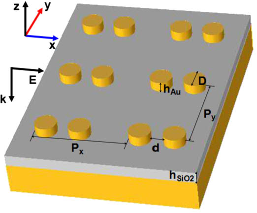
Fig. 2. (a) Simulated electric field intensity enhancement factors of the dimer grating (green solid line), the single disk grating (black square line), a single dimer (red circle line), and a single disk (blue triangle line) upon gold film separated by a layer of silica spacer. (b) Ez amplitude at position 2 for the gold dimer array case. (c) Schematics of the four structures simulated.

Fig. 3. (a) Intensity (| E | 2 h SiO 2 = 45 nm 2(a) , respectively.

Fig. 4. (a) Simulated electric field spectrum for the structure with P x = 550 nm P y = 500 nm d = 60 nm G SERS


Table1. Normalized Effective Mode Volume and the Quality Factor for Different Interparticle Separation Dimers, a Single Dimer with a Gap of 15 nm, and a Single Disk upon Gold Film Separated by a Layer of Silica Spacer
|
Zhengqing Qi, Jie Yao, Liangliang Zhao, Yiping Cui, Changgui Lu. Tunable double-resonance dimer structure for surface-enhanced Raman scattering substrate in near-infrared region[J]. Photonics Research, 2015, 3(6): 06000313.


 PDF全文
PDF全文

